What is LED PCB?
Understanding LED PCB
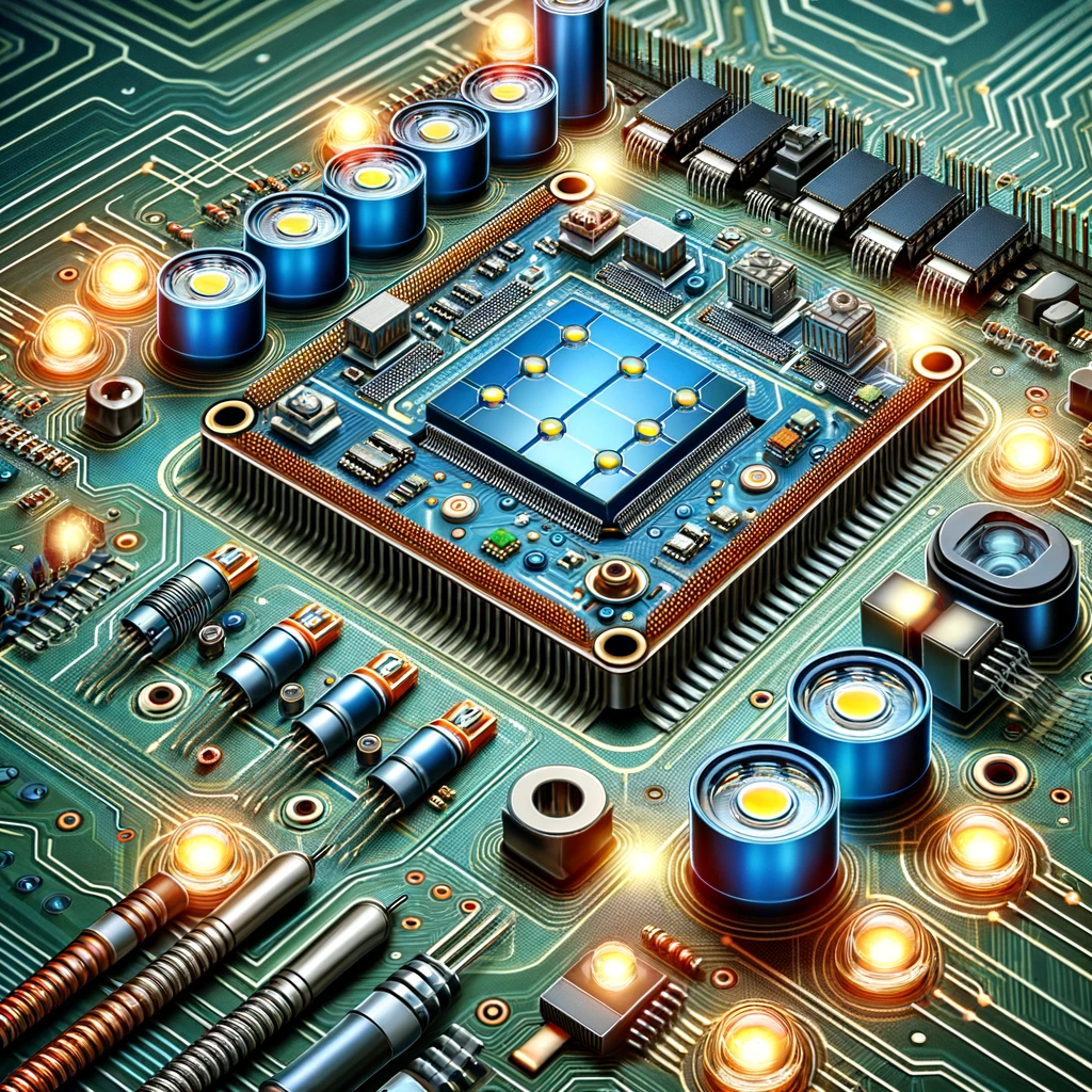
An LED PCB is specially designed to support and connect LED components in various electronic devices. Unlike traditional PCBs, LED PCBs are engineered to manage the higher heat output of LEDs, ensuring optimal performance and longevity. They are pivotal in enabling the efficiency and reliability of LED lighting systems.
Types of LED PCBs
- Single-Layer PCBs: These are the most basic form of LED PCBs, featuring a single layer of conductive material, typically used in simple lighting applications.
- Double-Layer PCBs: These boards have conductive copper layers on both sides, offering more flexibility in design and greater circuit density.
- Multi-Layer PCBs: Consisting of three or more layers of conductive material, these PCBs are used in complex lighting systems where space is limited and functionality demands are high.
- Aluminum Backed PCBs: Favoured for their ability to dissipate heat efficiently, these PCBs are ideal for high-power LED applications.
Key Components of LED PCBs
- Base Material: Typically, aluminum or copper, known for excellent thermal conductivity.
- Thermal Insulation Layer: A critical layer that manages heat, preventing damage to the PCB.
- Circuit Layer: Copper foil laminated onto the substrate, forming the pathway for electrical connections.
- Solder Mask: Protects the copper circuitry from short-circuiting, dust, and moisture.
- Silkscreen Layer: Adds labels and symbols on the PCB for easier assembly and troubleshooting.
Applications of LED PCBs
LED PCBs have found applications across a wide range of sectors due to their efficiency and durability. These include:
- Consumer Electronics: Smartphones, TVs, and wearable devices.
- Automotive Industry: Headlights, interior lights, and dashboard displays.
- Medical Devices: Surgical lighting and diagnostic equipment.
- Industrial Lighting: High bay lights, street lights, and floodlights.
- Aerospace and Military: Instrumentation lighting and cockpit displays.
Manufacturing Process of LED PCBs
The manufacturing of LED PCBs involves several precise and critical steps:
- Design and Layout: Utilizing CAD software to design the circuit layout.
- Material Selection: Choosing the appropriate base material and copper thickness.
- Circuit Printing: Applying a protective mask and etching away excess copper.
- Layer Pressing: For multi-layer PCBs, pressing layers together under high temperature and pressure.
- Drilling and Plating: Creating vias and plating them with copper for interlayer connections.
- Solder Mask Application: Applying a solder mask to protect and insulate the copper tracks.
- Silkscreen Printing: Adding labels for components and instructions.
- Assembly and Testing: Mounting components, soldering LEDs, and testing the finished PCB for functionality and reliability.
Benefits of LED PCBs
- Efficient Heat Dissipation: The use of aluminum and copper ensures effective heat management, crucial for LED performance.
- High Durability: LED PCBs are more robust and reliable, suitable for harsh environments.
- Energy Efficiency: They contribute to lower energy consumption in LED lighting solutions.
- Compact Size: Enables sleek and compact designs for modern electronic devices.
- Versatility: Suitable for a wide range of applications from consumer electronics to industrial lighting.
Challenges and Solutions
While LED PCBs offer numerous advantages, they also face challenges such as thermal management and higher manufacturing costs.
Advances in PCB design and materials, like improved thermal interface materials (TIMs) and cost-effective manufacturing techniques, continue to address these issues, making LED PCBs more accessible and efficient.
Future of LED PCBs
The future of LED PCBs looks bright, with ongoing innovations in materials, design, and manufacturing processes. Emerging trends include the use of flexible LED PCBs for wearable technology, the integration of smart technology for connected lighting solutions, and the development of environmentally friendly PCBs.
Conclusion
LED PCBs are at the heart of the revolution in lighting technology, offering unmatched efficiency, reliability, and versatility. As the demand for innovative and energy-efficient lighting solutions grows, LED PCBs will continue to play a pivotal role in shaping the future of electronics.
Whether in consumer gadgets, automotive lighting, or industrial applications, LED PCBs are lighting the way towards a brighter, more sustainable future.
Share:
More Posts

Humanizey Review: I Tested Everything Out
Humanizey Review: I Tested Everything Out AI writing tools have changed the way we create content. They’re fast, smart, and efficient. But even the best

AllPCB Review: Can We Trust It?
AllPCB Review: Can We Trust It? In this in-depth review, we’ll examine AllPCB’s strengths, weaknesses, and whether it deserves your trust. We’ll also explore PCBPit,

PCBgogo Review: Is It A Good PCB Manufacturer?
PCBgogo Review: Is It A Good PCB Manufacturer? In this in-depth review, we’ll dissect its strengths, weaknesses, and alternatives—with a focus on PCBPit, a rising

NextPCB Review: Does It Really Work?
NextPCB Review: Does It Really Work? Choosing a reliable PCB manufacturer is critical for bringing your electronics projects to life. NextPCB has been a prominent


