What Is PCB Insertion Loss?
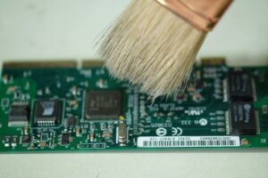
“Insertion loss” commonly denotes the diminution of signal intensity occurring as the signal traverses through the components and cabling at the system level, as well as the traces on printed circuit boards (PCBs) within systems operating at high speeds of 3GHz or more, including optical fibers and PCB stack-ups.
Often synonymous with “attenuation,” insertion loss quantifies the weakening of a signal as it is transmitted through an optical link or a transmission line. This value is generally represented in decibels (dB).
The Significance of Insertion Loss in PCBs
Insertion loss matters particularly at high frequencies, where it leads to signal attenuation and distortion. The signal experiences attenuation due to conductor resistance and leakage in the laminate material, while pulse distortion occurs when loss affects the signal harmonics unequally.
Since loss is dependent on frequency, higher harmonics face greater attenuation. The net effect is that the signal arriving at the load is a distorted version of the original, altering both amplitude and form.
Turn to PCBPit for all-in-one PCB solutions now >>
Catalysts of Insertion Loss in PCBs
For those new to RF systems, the concept of Wave can seem somewhat abstract. Yet, its design principles extend those employed in lower-frequency PCB designs. PCB insertion loss is primarily the result of variation in impedance along an interconnect. The measure of insertion loss quantifies the degree of signal degradation at points of impedance discontinuity.
- Copper Losses: Copper losses stem from the power dissipation that occurs due to conduction along the surfaces of connectors. This is typically an issue with the plating quality and material choice in the PCB.
- Dielectric Losses: Dielectric losses are due to power dissipation within the PCB’s dielectric materials.
- Reflective Losses: Reflective losses happen due to the connector’s voltage standing wave ratio (VSWR) along transmission lines. They occur when the load fails to absorb the power, leading to a reflection of energy back down the line.
For PCBs in the lower frequency spectrum, from 3Ghz to 5Ghz, impedance mismatch is the main culprit for signal loss. However, as we venture into much higher frequencies—10Ghz to 30Ghz and beyond—the dielectric constant, determined by the materials used, becomes the prominent issue causing insertion loss. Therefore, the selection of core materials, prepreg, and copper foil is critical when constructing the PCB stack-up.
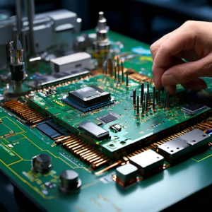
In Wave systems, vias often create the most disruption as they can introduce impedance discontinuity in impedance-controlled interconnects. Various via types—blind, buried, or through-hole—are used for layer transitions in multilayer PCB designs. These all come with parasitic elements that induce insertion loss at higher frequencies.
Examining a time-domain reflectometry trace of a Wave interconnect from a test coupon can sometimes reveal a capacitive impedance drop at plated through-hole vias for layer transitions. These impedance dips are problematic for two reasons. First, they cause reflections which can lead to standing waves and strong radiated EMI. Second, they reduce the level of signal that can reach the end-load, which is to say, they cause insertion loss.
Optimizing Insertion Loss in PCBs
Addressing insertion loss is fundamental when designing a high-speed PCB suited for your specific needs. Recognizing the root issues behind signal loss enables accurate selection of materials for stack-up, influencing glass weave tightness, resin density, and PCB thickness. Summarizing, consider the following when planning your PCB stack-up:
- Choose low-profile copper options, such as very low-profile ED copper or alternative oxide, to minimize skin effect and surface roughness.
- Opt for tighter fiberglass weaves for improved dielectric constants, or alternatively angle the copper traces over looser weaves to maintain signal integrity.
- Opt for materials that provide low dielectric constants and handle a broad range of signals smoothly through flat frequency responses.
- Use the materials with the least loss in dielectric properties and limit reach to limit dissipation factors.
Differing Considerations: Insertion Loss vs. Connector Return Loss
Connectors represent just one of the many elements in a transmission line of a multi-board system signal path, lying between the transmitter and receiver. In interconnect discussions, vias are often highlighted as inductive impedance disruptors. They resemble inductors at high frequencies and can cause reflections if not correctly designed. But connectors behave similarly, acting as miniature transmission lines with their own impedance which can affect signal interaction.
Despite the desire for flawless connectors, the reality is they do introduce return and insertion loss. This loss results from an impedance mismatch, mainly arising from surface mount pads on connectors. Through-hole connectors also contribute to insertion loss, with pins introducing inductive and capacitive impedance discrepancies.
SMD connector pads often increase per length capacitance when accompanied by wider copper, which consequently reduces the trace’s characteristic impedance at the connector pad. This capacitive impedance difference causes signal reflection, culminating in connector return loss and insertion loss.
Trends and Challenges in PCB Manufacturing for 2024
Trends and Challenges in PCB Manufacturing for 2024 As we move into 2024, the printed circuit board (PCB) manufacturing industry continues to evolve rapidly, driven
10 Best PCB Manufacturers in India
10 Best PCB Manufacturers in India The electronics manufacturing landscape in India has seen a significant transformation in recent years, with Printed Circuit Board (PCB)
Identifying PCB Components: A Step-by-Step Guide
Identifying PCB Components: A Step-by-Step Guide Printed Circuit Boards (PCBs) are the backbone of modern electronic devices, from simple gadgets to complex machinery. Knowing how
What is PCB in AC?
What is PCB in AC? Air conditioning has become an essential part of our daily lives, providing comfort and a conducive living environment regardless of