Introduction to Bare PCB Boards
A bare PCB board is a piece of material—typically fiberglass or composite epoxy—laminated with conductive pathways, pads, and other features etched from copper sheets.
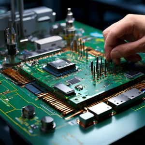
These boards provide the physical platform for mounting and interconnecting electronic components like resistors, capacitors, and integrated circuits through soldering.
Why Bare PCB Boards are Crucial
Bare PCBs are pivotal in defining the functionality, reliability, and performance of electronic devices. They serve not only as a base for component installation but also significantly influence the electrical performance of the assembled device.
The design and layout of the tracks, pads, and vias on a bare PCB determine the flow of electrical signals and power throughout the electronic system.
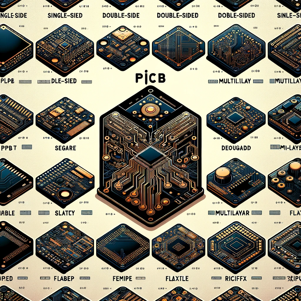
Types of Bare PCB Boards
Bare PCB boards come in various types, each suited to different applications based on their properties and the complexities of the electronic devices they support:
Single-Sided PCBs: These boards have one layer of conductive material, making them ideal for simple electronics where a compact size and low cost are paramount.
Double-Sided PCBs: With conductive layers on both sides, these PCBs offer more circuitry complexity without significantly increasing the size.
Multilayer PCBs: Comprising three or more layers of conductive material, multilayer PCBs support complex and high-density circuit designs, essential for advanced electronic systems.
Flexible PCBs: Made from materials that allow flexibility, these PCBs are used in applications where the board must conform to a particular shape or withstand frequent bending.
Rigid-Flex PCBs: Combining features of both rigid and flexible PCBs, these are used in sophisticated electronic products that require durability and flexibility.
The Manufacturing Process of Bare PCB Boards
The manufacturing process of bare PCB boards is intricate and involves several steps, each critical to the board’s final quality and functionality:
Design and Layout: Utilizing specialized software, engineers design the PCB layout, including the placement of tracks, pads, and vias.
Material Preparation: The chosen substrate material is prepared, cut to size, and cleaned to ensure optimal adhesion of the conductive layers.
Circuit Pattern Transfer: The circuit design is transferred onto the substrate using either a photolithographic process or a mechanical milling process.
Etching: Unwanted copper is removed from the substrate, leaving behind the desired circuit pattern.
Drilling: Holes and vias are drilled into the board to allow electrical connection between different layers or components.
Plating and Coating: The board may undergo various plating processes to enhance conductivity, solderability, and resistance to oxidation.
Testing: Each board is tested for electrical functionality and adherence to design specifications.
Applications of Bare PCB Boards
Bare PCB boards are ubiquitous in the electronics industry, finding applications in virtually every sector:
- Consumer Electronics: Smartphones, computers, and home appliances rely on PCBs for their electronic circuits.
- Medical Devices: From wearable health monitors to complex diagnostic equipment, PCBs are crucial in medical technology.
- Automotive Industry: Modern vehicles use PCBs for everything from engine control units to infotainment systems.
- Industrial Machinery: PCBs control and monitor industrial equipment, ensuring precision and reliability in manufacturing processes.
- Aerospace and Defense: High-reliability PCBs are used in critical applications, from satellite communications to flight control systems.
Key Considerations in Bare PCB Board Design
When designing a bare PCB board, several factors must be considered to ensure the final product meets its intended performance criteria:
- Material Choice: The substrate material affects the PCB’s thermal resistance, mechanical strength, and electrical properties.
- Circuit Complexity: The design must accommodate the circuit’s complexity within the space constraints, considering the number of layers and routing density.
- Thermal Management: Effective design includes considerations for heat dissipation to prevent overheating of components.
- Signal Integrity: The layout should minimize electromagnetic interference and signal loss, ensuring reliable operation.
- Manufacturability: The design must be feasible for manufacturing, considering aspects like board thickness, hole sizes, and tolerances.
Conclusion
Bare PCB boards are at the heart of electronic innovation, offering a canvas on which the modern world’s technological advancements are painted. Understanding the types, manufacturing processes, applications, and design considerations of these boards is crucial for anyone involved in electronics design and manufacturing.
As technology continues to evolve, the role of the bare PCB board will only grow, underlining the need for continual innovation and expertise in this foundational element of the electronics industry.
Trends and Challenges in PCB Manufacturing for 2024
Trends and Challenges in PCB Manufacturing for 2024 As we move into 2024, the printed circuit board (PCB) manufacturing industry continues to evolve rapidly, driven
10 Best PCB Manufacturers in India
10 Best PCB Manufacturers in India The electronics manufacturing landscape in India has seen a significant transformation in recent years, with Printed Circuit Board (PCB)
Identifying PCB Components: A Step-by-Step Guide
Identifying PCB Components: A Step-by-Step Guide Printed Circuit Boards (PCBs) are the backbone of modern electronic devices, from simple gadgets to complex machinery. Knowing how
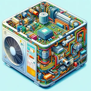
What is PCB in AC?
What is PCB in AC? Air conditioning has become an essential part of our daily lives, providing comfort and a conducive living environment regardless of