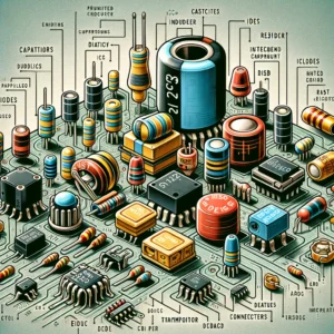
What Is A PCB Pad?
A PCB pad refers to the exposed copper area on a circuit board, where the component lead is soldered. All electrical connections of the components are established through the pads. The design and placement of pads play a critical role in the solderability, stability, and heat transfer of the components.
Based on the specific components and packaging methods, PCB pads are typically categorized as through-hole pads and surface mount pads.
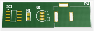
Surface Mount Pads
Pads that enable electronic components to be directly mounted on the board surface are referred to as surface mount pads. Unlike through-hole pads, surface mount pads are well-suited for mounting smaller components. They allow for a greater number of components to be accommodated within a smaller space while simultaneously delivering enhanced functionality and performance.
This type of pad presents a significant advantage in the design of complex multi-layer boards. Nonetheless, surface mount pads are not typically suitable for components that generate high levels of heat.
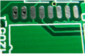
Through-Hole Pads
Pads utilized for mounting through-hole components are known as through-hole pads. During the soldering process, the component pins must be inserted into the via holes of the pad.
Soldering components via through-hole pads ensures reliable solder joints between the components and the PCBs, establishing durable mechanical and electrical connections over time. However, the presence of component leads and the number of holes may limit the available routing areas on a multilayer board.
BGA Pads
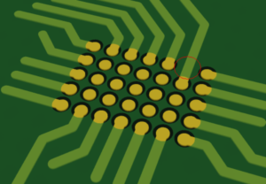
When connecting BGA-style components, the appropriate pad design is crucial for ensuring the manufacturability of the boards. Two common types of BGA pads are Solder Mask Defined Pads (SMD) and Non-Solder Mask Defined Pads (NSMD).
Solder Mask Defined Pads (SMD)
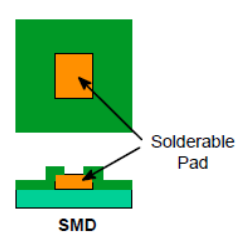
SMD pads are defined by the solder mask apertures applied to the BGA pads. In this pad design, the mask aperture is smaller than the actual copper pad, and the pad is partially covered by the surrounding solder mask. The use of SMD pads offers certain advantages, such as preventing the pad from shifting or detaching from the board due to overlapping mask. Additionally, the pad facilitates BGA positioning.
However, this type of pad reduces the contact area between the pad and the copper surface, as well as the space between adjacent pads, which limits the thickness of the tracks between the pads and can impact the use of through-holes.
Non-Solder Mask Defined Pads (NSMD)
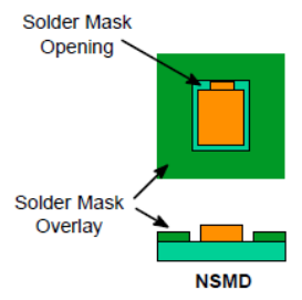
NSMD, short for Non-Solder Mask Defined Pad or Copper Defined Land Pattern, is characterized by the size of the pad being defined by the diameter of the pad itself rather than the solder mask aperture. There is a small gap between the edge of the pad and the solder mask, and the pad is independent with the copper on the surface being fully exposed.
This pad design provides a larger surface area for solder joint connections, offering greater clearance between pads, and is widely utilized in high-density and fine-pitch BGA chips. A drawback of NSMD pads is their susceptibility to delamination caused by thermal and mechanical stresses.
Conclusion
Pads play a significant role in the pattern and fabrication of PCB pads. Mastering this aspect is crucial for circuit board designers in creating fully operational and efficient electric circuit boards. Remember you can always turn to PCBPit for one-stop PCB solutions.
Trends and Challenges in PCB Manufacturing for 2024
Trends and Challenges in PCB Manufacturing for 2024 As we move into 2024, the printed circuit board (PCB) manufacturing industry continues to evolve rapidly, driven
10 Best PCB Manufacturers in India
10 Best PCB Manufacturers in India The electronics manufacturing landscape in India has seen a significant transformation in recent years, with Printed Circuit Board (PCB)
Identifying PCB Components: A Step-by-Step Guide
Identifying PCB Components: A Step-by-Step Guide Printed Circuit Boards (PCBs) are the backbone of modern electronic devices, from simple gadgets to complex machinery. Knowing how
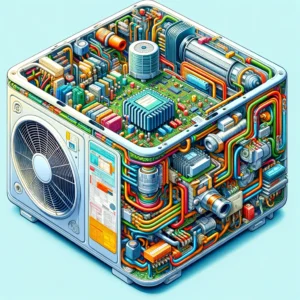
What is PCB in AC?
What is PCB in AC? Air conditioning has become an essential part of our daily lives, providing comfort and a conducive living environment regardless of