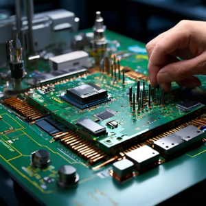
Introduction to PCB Fiducial Mark
Fiducial marks play a crucial role in PCB assembly, functioning as reference points for automated machines and ensuring precise placement of components on the board.
These marks, usually in the form of circular pads surrounded by clearance areas, are detected by computer vision systems, enabling accurate alignment. There are two primary types of fiducial marks—global and local—tailored to different requirements within the PCB assembly process.
There’re two PCB fiducial marks, let’s explore them in the following part.

Global Fiducial Marks: Enhancing Precision
A crucial aspect of the PCB manufacturing process involves the placement of global fiducial marks, often referred to as panel fiducials. These are typically located near the corners of the PCB or along the panelization rails. The decision of where to position these markers is driven by a strategy derived from years of understanding the complex dynamics around PCB assembly. A well-placed panel fiducial ensures a smooth ergonomic relationship between the PCB and the machinery used in assembly, thereby maximizing efficiency and accuracy.
These marks are not placed arbitrarily; instead, they serve a critical role to optimize the alignment of multiple PCBs during assembly. This alignment is pivotal in ensuring the right connections and placements of components on the board. Consequently, proper fiducial marking contributes significantly to the overall accuracy of the assembly, reducing errors and enhancing the performance of the final product. This results in a seamless integration of different electronic components, leading to highly efficient and high-performance electronic products.
Local Fiducial Marks: Precision in High-Density Areas
On the other hand, local fiducial marks, as compared to their global counterparts, are notably smaller and nestled within the precincts of dense component clusters or intricate routing locations on the PCB. Their reduced size doesn’t impede their functionality; rather, it’s a critical trait that allows them to be accommodated in areas where real estate on the PCB is at a premium. The placement of these marks is thoughtfully strategized, often found neighboring high-precision components or areas featuring complex routing structures.
The primary objective of local fiducial marks is to ensure pinpoint accuracy in component placement within these densely populated or complex sections of the board. They achieve this by acting as a reliable reference point for the machinery to recognize the exact locations where components need to be placed. Such precision is especially crucial for components like BGAs and QFNs, where inaccurate placement can lead to manufacturing defects and impact the performance of the final product. Hence, while they may seem like a minute detail, local fiducial marks play a tremendous role in enhancing the overall productivity and efficiency of the PCB assembly process.
The Purpose of Fiducial Marks
Fiducial marks, both global and local, stand as reliable landmarks amidst the intricate landscape of a PCB. Their distinct shapes and patterns make them easily recognizable, setting them apart from other patterns, holes, or components on the board. The recognition of these fiducials is incredibly important for the automated machines used in PCB manufacturing, allowing them to identify specific regions of the PCB. Functioning like an advanced version of a ‘You are here’ marker on a map, these fiducial marks orient the machines to their precise location on the board.
Given their standardized shapes and sizes, their recognition within the system is streamlined, with less room for error in identification. The consistency in dimensions and positioning of fiducial marks across different PCB designs builds a universal language that machines can easily interpret. This standardization lends itself to ensuring consistent alignment during the assembly process. Each component finds its designated place accurately, irrespective of the complexity of the design or the density of components on the board.
In summary, fiducial marks, through their standard shape, size, and placement, serve as the guiding stars, navigating automated machines throughout the assembly process, ensuring precision, and contributing greatly to the overall efficiency and success of the PCB manufacturing process.
Key Guidelines for Fiducial Mark Usage
When incorporating fiducial marks into PCB designs, several crucial guidelines should be observed. These include maintaining consistent diameter throughout the design for accurate alignment, incorporating marks on both sides of the PCB for comprehensive assembly, and ensuring that the marks remain free from solder masks and coatings to guarantee visibility and detectability.
By adhering to these guidelines and fully understanding the role of fiducial marks, PCB designers can enhance the accuracy and efficiency of the assembly process, ultimately leading to high-quality end products.
Trends and Challenges in PCB Manufacturing for 2024
Trends and Challenges in PCB Manufacturing for 2024 As we move into 2024, the printed circuit board (PCB) manufacturing industry continues to evolve rapidly, driven

10 Best PCB Manufacturers in India
10 Best PCB Manufacturers in India The electronics manufacturing landscape in India has seen a significant transformation in recent years, with Printed Circuit Board (PCB)

Identifying PCB Components: A Step-by-Step Guide
Identifying PCB Components: A Step-by-Step Guide Printed Circuit Boards (PCBs) are the backbone of modern electronic devices, from simple gadgets to complex machinery. Knowing how

What is PCB in AC?
What is PCB in AC? Air conditioning has become an essential part of our daily lives, providing comfort and a conducive living environment regardless of