
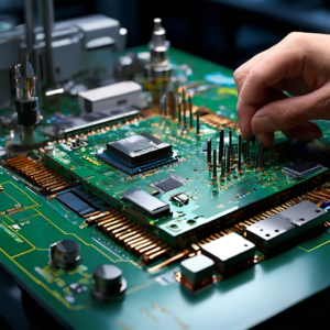
Trends and Challenges in PCB Manufacturing for 2024
Trends and Challenges in PCB Manufacturing for 2024 As we move into 2024, the printed circuit board (PCB) manufacturing industry continues to evolve rapidly, driven
Essential to all major electronic devices, Printed Circuit Boards (PCBs) are found in an array of digital products, including simple items like clocks, calculators and such. For those unfamiliar, PCBs control electrical signals within electronic products to meet the device’s electrical and mechanical circuit needs. To put it simply, PCBs dictate the direction for electricity, giving life to your electronic devices.
PCBs manage electric current across their surface via a network of copper routes. The intricate matrix of copper pathways characterizes the specific function of each section of the PCB circuit board.
Ahead of the PCB design phase, circuit designers are advised to visit a PC board shop and consult with manufacturers face-to-face about their PCB production needs. This approach can eliminate potential unnecessary errors in the design phase. However, as most companies offshore their PCB production queries to international suppliers, this approach becomes impractical. As such, we present this article to give you an adequate understanding about steps involved in PCB board manufacturing. We hope it offers circuit designers and newcomers to PCB Industry a transparent perspective on how printed circuit boards are produced, and aids in avoiding unnecessary mistakes.
PCB layouts, planned by the designer using PCB design software, should be stringently compatible with circuit boards. Altium Designer, OrCAD, Pads, KiCad, Eagle etc. are commonly used PCB design software. NOTE: Prior to PCB production, designers must notify their contract manufacturer about the PCB design software version utilized to craft the circuit as it aids in mitigating issues caused by inconsistencies.
Post approval for PCB design for production, designers transmute the design into a format endorsed by their manufacturers. The most widely used program is extended Gerber. The 1980’s baby food ad campaign sought attractive infants, and this software generates eloquently designed progeny. Gerber is also known as IX274X.
Extended Gerber became recognized as the optimal output format in the PCB industry. Various PCB design software may demand different Gerber file generation steps, but all encode pivotal information including copper tracking layers, drill drawing, apertures, component notations and other settings. Every element of the PCB design is inspected at this stage. The software applies oversight algorithms to the design to ensure no error goes unnoticed. Designers also scrutinize the design considering elements related to track width, board edge spacing, trace and hole spacing, and hole size.
Post rigorous examination, designers pass the PCB file to PC Board Houses for production. To guarantee the design meets requirements for the minimum tolerances during the production process, nearly all PCB Fab Houses conduct a Design for Manufacture (DFM) check preceding the fabrication of circuit boards.
PCB printing begins once designers output the PCB schematic files and manufacturers carry out a DFM check. Manufacturers employ a unique printer called a plotter to create photographic films of the PCBs, which are then used to print circuit boards. Although it’s technically a laser printer, it isn’t a standard laser jet printer. Plotters utilize extraordinarily precise printing technology to render a highly detailed film of the PCB design.
The final output is a plastic sheet with a photo negative of the PCB in black ink. For the inner layers of PCB, black ink signifies the conductive copper sections of the PCB. The remaining clear portion of the image represents the areas of non-conductive material. The external layers follow the reverse arrangement: clear stands for copper, while black characterizes the area to be etched away. The plotter auto-develops the film, and the film is securely stored to prevent any accidental contact.
Each layer of PCB and solder mask gets its own individual clear and black film sheet. In sum, a two-layer PCB demands four sheets: two for the layers and two for the solder mask. Importantly, all the films must match perfectly to each other. If used together, they layout the PCB alignment.
To ensure immaculate alignment of all films, registration holes are to be punched through all films. The precision of the hole transpires by adjusting the table upon which the film rests. Once the minute adjustments of the table lead to an ideal match, the hole is punched. The holes will align with the registration pins in the next step of the imaging process.
Step 3: Printing the Inner layers: Where should the copper go?
The goal of creating films in the preceding step was to layout a blueprint of copper track. Now, the image on the film should be printed on a copper foil.
The procedure of fabricating a PCB first prepares for the actual creation of the PCB. The basic PCB setup begins with a laminate board, consisting of epoxy resin and glass fiber, also known as substrate material. The laminate functions well as a recipient for the copper that outlines the PCB. The robust and dust-resistant substrate material serves as an excellent launching pad for the PCB. Copper is previously adhered on either side. The progression involves carving out the copper to uncover the blueprint from the films.
Maintaining cleanliness is pivotal in PCB formation. The copper-inclusive laminate gets cleaned and transported into a sterilized zone. At this phase, it’s crucial that no contaminants compromise the laminate surface. If overlooked, a mere particle of dust may unleash a circuit short or stay open.
Following this, the freshly cleaned panel gets introduced to a photo-sensitive coating named photo resist. This layer incorporates a series of chemicals reactive to light, which toughen when exposed to UV light. This guarantees an exact correlation from the photo films to photo resist. The films are positioned onto pins that maintain their position over the laminate board.
The film and panel synchronize and become subjected to UV light. This light illuminates the transparent film sections, solidifying the photo resist on the underlying copper. The plotter’s black ink averts light from reaching areas deemed to stay soft, signifying their removal.
Once the board preparation concludes, an alkaline solution is applied to wash off any remaining unhardened photo resist. A concluding pressure wash eliminates potential residual matter on the surface before the board gets dried.
The end is a product with resist suitably layered over the copper segments intended to be part of the final artifact. A technician scrutinizes the boards verifying no missteps during this phase. The resist present at this juncture signifies the copper that will show up in the completed PCB.
This phase is applicable only to boards with over two layers. Basic two-layer boards leap onto the drilling stage. Boards with multi-layers necessitate additional steps.
With the photo resist stripped and the solidified resist guarding the aimed copper, the board moves to removing undesired copper. Similar to how the alkaline solution removed the resist, a potent chemical blend dissolves the excessive copper. The copper solvent solution bath wipes off all bare copper. Meanwhile, the targeted copper stays heavily shielded under the photo resist’s hardened layer.
Different copper boards possess different standards. Heavier boards might need larger volumes of copper solvent and variable exposure durations. Notably, heavier copper boards demand extra focus on track spacing. Majority of standard PCBs hinge on the same specification.
Once the solvent has obliterated nonessential copper, it’s time for the hardened resist protecting the prioritized copper to be washed off. Another solvent achieves this. The board then sparkles with just the copper substrate required for the PCB.
With the layers pristine and prepared, they need punch holes for alignment. To line up inner layers to the outer ones, registration holes are necessary. To ensure precise correspondence, the technician places the layers onto a device known as the optical punch; this is where the accurate punching of registration holes occurs.
A secnd device performs an automatic optical inspection to spot potential defects when the layers are assembled, as corrections are unattainable afterwards. The originating design from Gerber, given to the manufacturer, acts as the reference. This machine scans the layers with a laser sensor and electronically juxtaposes the digital image with the original Gerber file.
If inconsistencies are noticeable, these displays on a screen for the technician to evaluate. The layer, if cleared during inspection, advances to the concluding stages of PCB manufacturing.
The circuit board starts taking shape at this juncture. All the isolated layers queue for their interconnection. With the layers accounted for and verified, the only task left is their integration. The outer layers have to consociate with the substrate within two steps: layer-up and bonding.
The outer layer material is sheets of fiber glass, previously imbued with epoxy resin, otherwise known as prepreg. A copper film also blankets the top and bottom of the original substrate housing the copper trace etchings. The time has come for these materials to be pressed together.
The bonding takes place on a heavy steel table using metal clips. The layers are securely set onto pins on the table. Everything is pressed snugly together to prevent displacement during alignment.
Initially, a prepreg sheet is positioned over an alignment basin by a technician. A substrate layer is carefully laid on the prepreg, followed by a copper sheet. Additional prepreg layers are arranged on the copper sheet before ending with a copper press plate and an aluminum foil. The entire assembly is then set up for pressing.
Controlled by the computer of the bonding press, the entire procedure goes through an automatic sequence. It directs the heating of the assembly, when to apply the necessary pressure, and when to permit the stack to cool steadily.
Afterwards, there is a bit of deconstruction. The multi-layered PCB, which has all the layers fused into one amazing sandwich, is efficiently unpacked by the technician. This involves removing the restraining pins and disposing of the top pressure plate, unveiling the PCB housed within its aluminum press plates shell. The copper foil used in this process serves as the external layers of the PCB.
Subsequently, precise holes are carved into the stack board. The forthcoming components such as copper-connected via holes and leaded segments are dependent on the accuracy of these drill holes – so fine that the drill achieves a width of 100 microns compared to an average hair width of 150 microns.
The x-ray locator determines the accurate drill targets before proper registration holes are made to stabilize the stack board for the subsequent specific holes.
Pre-drilling involves setting a buffer material board beneath the drill target to ensure a clean drill. An exit-material deters any unnecessary tearing when the drill exits. Each micro-move of the drill is regulated by a computer. It uses the digital file from the initial design to identify where to drill.
Air drives the drill spindles at a whirling 150,000 rpm. Despite this speed, drilling takes its time due to the numerous holes to make. Later, these cavities accommodate the vias and mechanical mounting holes of the PCB, with their final attachment happening post plating.
Once drilling is completed, additional copper lining the production panel’s edges is removed by a profiling tool.
Post-drilling, the panel proceeds to plating. Chemical deposition fuses the various layers during this process. Following thorough cleansing, the panel enters a sequence of chemical baths which dishes out a thin layer of copper of about one micron onto the panel surface. This copper enters the newly drilled holes.
Previously, the interior hole surfaces simply revealed the comprising fiber glass material of the panel interior. The copper baths uniformly plate the hole walls. Consequently, a new copper layer is formed on the panel, most notably covering the new holes. Computers oversee the entire dipping, removal, and procession procedure.
Remember Step 3 where we used photoresist on the panel? It’s time to do it again, but this time the outer layers are imaged with the PCB design. The procedure begins under sterile conditions to avoid any particles sticking to the layer surface. A layer of photo resist is then applied to the panel. The panel, now prepared, progresses into the yellow room where UV lights, harmful to photoresist, are notably absent due to yellow light wavelengths.
Black ink transparencies are firmly held by pins to avoid misplacement with the panel. Once panel and stencil make contact, they’re subjected to intense UV light causing the photo resist to harden. Following this, a machine strips away the unhardened resist that was protected by the opacity of the black ink.
This process is essentially the opposite of the one used on the internal layers. Lastly, the outer plates are inspected to ensure all unwanted photo resist was removed in the previous stage.
Transitioning back to the electroplating section, we proceed in the same way as detailed in Step 8, coating the panel with a thin copper layer. The panel sections uncovered during the previous photo resist step undergo electro-plating. The panel typically undergoes an initial set of copper plating baths before progressing to tin plating. This facilitates the removal of any residual copper slated for elimination. The tin layer plays a crucial role in shielding the portion of the panel intended to remain copper-coated throughout the subsequent etching phase. The etching process eliminates any superfluous copper foil from the panel.
The protective tin layer safeguards the necessary copper during this phase. The copper elements not required and that underneath the remaining resist layer are stripped away. Once more, chemical treatments are employed to get rid of the surplus copper while the tin layer continues to protect the vital copper portions.
At this stage, all conducting areas and connections are correctly established.
The panels are cleansed prior to the application of the solder mask, and then coated with an epoxy solder mask ink on both sides. The panels are exposed to UV light through a solder mask photo film, leaving the covered areas in an uncured state ready for removal.
Finally, the board is placed in an oven to fix the solder mask.
Chemical plating with gold or silver is applied to the PCB for enhanced solder-ability. Certain PCBs also undergo hot air leveling at this phase, resulting in uniform pads and creating the surface finish. PCBPit offers a variety of surface finishing techniques as per customer requirements.
The board nears completion with the application of ink-jet writing indicating all crucial PCB details — the PCB then moves on to the final coating and curing process.
To ensure functionality and alignment with original design, a comprehensive electrical test of the PCB is undertaken by a technician. PCBPit offers the enhanced Flying Probe Testing which uses mobile probes to test each bare circuit board’s electrical performance.
The ultimate step involves sectioning different boards from the master panel using either a routing or v-groove technique. While routing leaves tiny tabs along the board boundaries, v-grooving slices diagonal channels on either side of the board. Both methods allow for easy removal of boards from the panel.
As evident, the PCB production process requires substantial effort. To ensure your PCBs meet your quality, performance, and durability standards, choosing a manufacturer with top-tier expertise, focusing on quality throughout all stages is essential.
PCBPit, one of China’s premier custom PCB production providers, commits to success by putting our clients’ success front and center in our operations. Every fabrication step receives utmost attention to detail. We offer additional services like vacuum packaging, weighing, and safe delivery, guaranteeing your PCB order arrives damage-free. Having serviced numerous businesses across 80 countries, our vision is to deliver our manufactured PCBs globally.
Our services encompass quickturn PCB prototyping, mass PCB production, and assembly. Rapid and FREE quotations are always available.
Trends and Challenges in PCB Manufacturing for 2024 As we move into 2024, the printed circuit board (PCB) manufacturing industry continues to evolve rapidly, driven
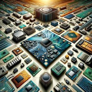
10 Best PCB Manufacturers in India The electronics manufacturing landscape in India has seen a significant transformation in recent years, with Printed Circuit Board (PCB)
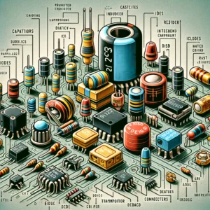
Identifying PCB Components: A Step-by-Step Guide Printed Circuit Boards (PCBs) are the backbone of modern electronic devices, from simple gadgets to complex machinery. Knowing how
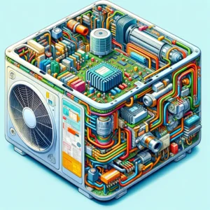
What is PCB in AC? Air conditioning has become an essential part of our daily lives, providing comfort and a conducive living environment regardless of

At PCBPit, we're experts in PCB aiming to provide the best PCB manufacturing services. Please reach out to discuss your needs.
Company
Get In Touch