Introduction
Flexible printed circuit boards (PCBs), commonly referred to as flex circuits, offer unique capabilities beyond traditional rigid PCB technologies. Their flexible construction allows them to bend, fold, and flex dynamically in use, making them essential in modern electronic devices and products due to increasing miniaturization and innovation in electronics.
Understanding the fundamentals of flexible PCB technology will help you determine the effective utilization of flex circuits in your electronic products and designs. You can turn to PCBPit – the trusted PCB manufacturing company for flex PCB solutions.
What is a Flex PCB?
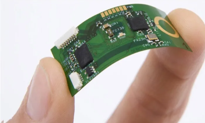
A flexible PCB utilizes a dielectric base layer made of a flexible polymer material such as polyimide or polyester. Conductive copper traces are laminated onto the flexible base layer to create a thin, bendable circuit board. The absence of rigid fiberglass reinforcement allows the flex PCB to be dynamically flexed and contorted during use.
Common names used to refer to flexible PCBs:
- Flex circuits
- Flexible circuits
- Flexible printed circuits
- Flex prints
Key properties that distinguish flex PCBs include their flexibility, lightweight nature, dynamic behavior, durability, integration with components, space-saving design, and customizability. These capabilities enable flexible circuits to meet the complex physical and electrical demands in compact, portable electronic devices.
Flexible PCB Materials and Construction
The unique materials and construction of flexible PCBs enable their distinct capabilities. The key components of a flex circuit’s build are:
Dielectric Flexible Substrate
The base dielectric layer provides the foundation upon which the conductive traces are fabricated. Selecting the appropriate flexible substrate material is crucial.
Common options include polyimide (Kapton), polyester (PET), polyamide, fluoropolymers (PTFE), and Liquid Crystal Polymer (LCP). Polyimide is the most widely used flex substrate material due to its high durability, thermal properties, and cost-benefit ratio.
Copper Foil
An ultrathin rolled annealed copper foil is laminated onto the base substrate. Typical foil thickness in flex PCBs ranges from 12μm to 35μm (0.5 oz to 1 oz).
Conductors
The copper foil is patterned using lithographic processes to produce the required conductive paths or traces.
Coverlay
A thin flexible dielectric coverlay can be laminated over the conductor layer for insulation and protection.
Bonding Adhesive
Acrylic or epoxy-based adhesive films are used to bond the base substrate with copper foil and coverlay with conductors.
Stiffeners
Additional dielectric stiffening layers may be added in multilayer constructions to minimize flex PCB wrinkling or buckling due to thermal stresses.
Finish and Coatings
A solder mask coats the conductor pattern for insulation and anti-oxidation. Hot air solder leveling (HASL) or other surface finishes can be applied to exposed pads.
Key Properties of Flexible PCBs
The materials and construction methods impart characteristic properties to flex circuits, including overall thickness, bend radius, heat resistance, chemical resistance, and lightweight nature. These properties make flex PCBs well-suited for a wide range of electronic applications.
Characteristics of Flexible PCBs
- High Frequency Properties – Short signal paths and thin dielectric materials contribute to excellent high frequency performance. Substrates such as LCP offer superior RF properties, making them suitable for high frequency applications.
- Current Ratings – The current carrying capacity of flexible PCBs is limited by copper thickness, with typical continuous current ratings ranging from approximately 0.5A to 5A for common flex circuit constructions.
By carefully selecting materials and adhering to design rules, the properties of flexible PCBs can be tailored to meet specific application requirements.
Considerations for Flexible PCB Design
Designing a dependable flex PCB requires special attention to dynamic bending aspects. The following are key guidelines to consider:
- Trace Width and Spacing – Narrower traces necessitate increased flex spacing to prevent cracks. A recommended 2:1 ratio of spacing to trace width is advisable for dynamic regions.
- Bend Radius – Routing traces perpendicular to bend axes is essential. It is important to maintain a bend radius of at least 3X the base thickness for static regions and 10X for dynamic bend regions.
- Coverlay Voids – To prevent wear, coverlay voids should be minimized in areas where traces are exposed. Strategic placement of voids should be considered in dynamic bend zones.
- Reinforcement – Additional stiffeners may be required in multilayer regions to prevent buckling and wrinkling during bending.
- Adhesives – Utilize high performance flexible adhesives designed for dynamic flex applications. Acrylic adhesives are known for their durability.
- Vias – Tear-drop shaped vias with adequate annular rings should be used to prevent crack propagation from the drill hole edges.
- Corners – Rounding sharp trace corners with higher radii helps reduce stress concentrations. It is advisable to avoid angled traces at corners.
- Pads – Implement rounded rectangle shaped pads or circles. Pads at flexing areas should be thermally relieved with neckdowns.
- Shielding – Flexible shielding films or conductive layers aid in EMI/ESD protection. Dedicated shielding traces can also be integrated.
By adhering to these specialized guidelines, flex PCBs can be designed to endure millions of flexing cycles and have long product lifetimes.
Common Types and Applications of Flex PCBs
Flexible circuits can be utilized in various configurations for interconnect and packaging applications:
- Flexible Interconnects – Simple conductor traces or wire patterns are used over flexible substrates to connect PCBs, displays, and other modules over dynamic movements.
- Flexible Cables – Utilize parallel conductor traces over rolled flex substrates to create high-density ribbon cables for signal, data, and power interconnections.
- Membrane Switches – Integrate conductor traces, spacers, and flexible overlays to produce ultra-thin touch sensitive control switches.
- Flex Rigid Boards – Incorporate rigid boards with flexible sections to create compactly foldable hybrid PCBs with complex rigid portions.
- Flexible Heaters – Pattern resistive heating elements on flex substrates to create thin heating pads and blankets capable of conforming to surfaces.
Some common applications of flex PCBs include medical instruments, wearable devices, robotics and industrial machines, consumer electronics, automotive electronics, aerospace and military systems. The flexibility, light weight, and dynamic characteristics of flex circuits enable innovative design possibilities.
Advantages of Flex PCBs
Flexible PCB technology offers several key benefits:
- Dynamic Flexing – Can endure millions of movement cycles, enabling rolling, twisting, and folding which is not feasible with rigid PCBs.
- Conforms to Shape – Can tightly integrate with product contours and housings unlike rigid boards.
- Lightweight – Exhibits extremely low mass compared to rigid laminates, making it suitable for portable and wearable devices.
- Thin Form Factor – Enables the creation of compact, low-profile circuits to fit small spaces and facilitate thinner products.
- Durable – Resistant to vibrations and mechanical shocks due to its flexible construction.
- High Density – Integrates interconnects, eliminating the need for external cables and connectors.
- Custom Shapes – Can be manufactured in unlimited 2D shapes and outlines.
- Soft and Pliable – Allows for the integration of complete electronic systems into fabrics.
- Reliability – Offers consistent performance over flex life with proper design.
- Cost Savings – Simplifies assembly, reduces the need for connectors, and lowers total product cost.
Challenges and Limitations
While offering numerous advantages, flexible PCB technology also presents the following limitations:
- Limited Layers and Density – Typically allows for 1-6 layers, restricting the complexity of circuits. High density multilayer flex is still under development.
- Lower Current Ratings – Copper thickness limits current carrying capacity, typically under 5A.
- Challenging Assembly – Requires specialized SMT processes suitable for flexible substrates.
- Prone to Wear – Improper dynamic flex spacing may lead to cracks and conductor failures.
- Backing Structure Requirement – Flex circuits must be assembled onto rigid frames or enclosures for complete system integration.
- Thermal Management Concerns – The insulating polymer substrate hinders heat dissipation.
- Susceptible to Environmental Damage – Requires additional protective encapsulation to mitigate environmental damage.
With sound design practices and advancements in materials, ongoing efforts are being made to address these limitations and expand the capabilities of flex PCBs.
Comparison of Flexible PCBs and Rigid PCBs
While rigid PCB technology is suitable for many applications, in certain cases transitioning to flexible PCB implementation is advantageous. The following presents a comparison between flexible PCBs and rigid PCBs:
Parameter Flexible PCB Rigid PCB Composition Polymer dielectric (PI, PET) Rigid laminate (FR4) Layers Typically 1-6 layers Up to 30+ layers Features Fine line traces, small vias Allows ultra-fine features (<3 mil) Density Medium density Very high density possible Thermal Conductivity Poor conduction through polymer Good thermal conduction Current Capacity Typically < 5A High currents possible Assembly Requires specialized SMT process Standard SMT assembly Shape Can produce any 2D contour Limited to rectangular boards Bend Radius Can flex dynamically Almost no bend radius Cost $$ $$$
While rigid PCBs serve most high complexity, density, and power applications, flex PCBs provide the mechanical flexibility needed in space restricted mobile designs. The optimal solution is often integrating both on a rigid-flex PCB to leverage the best of both technologies.
Future Trends in Flexible PCBs
Here are some key trends shaping the continued evolution of flexible PCB technology:
- Thinner Constructions – Reducing flexible layer thicknesses down to 1 mil to improve bendability.
- Smaller Features – Narrower trace widths and spacing down to 2 mils to increase integration.
- Improved Materials – New substrates like LCP for better electrical and high frequency performance.
- Fine Pitch Components – Enabling direct surface mount of ultra-fine pitch ICs on flex PCBs.
- High Density Flex – Development of flexible multilayer boards up to 12 conductive layers.
- Embedding Passives – Incorporating thin embedded resistors and capacitors within the flexible layers.
- Stretchable Circuits – Adopting novel materials to allow flexible PCBs to stretch and deform.
- Additive Processing – Transitioning from subtractive etching to additive fabrication using printing or plating processes.
- 3D Structured Flex Circuits – Techniques to fabricate out-of-plane flex circuit structures.
As material science and manufacturing processes mature, flex PCB technology will open doors to more innovative electronics designs not feasible before.

AllPCB Review: Can We Trust It?
AllPCB Review: Can We Trust It? In this in-depth review, we’ll examine AllPCB’s strengths, weaknesses, and whether it deserves your trust. We’ll also explore PCBPit,

PCBgogo Review: Is It A Good PCB Manufacturer?
PCBgogo Review: Is It A Good PCB Manufacturer? In this in-depth review, we’ll dissect its strengths, weaknesses, and alternatives—with a focus on PCBPit, a rising

NextPCB Review: Does It Really Work?
NextPCB Review: Does It Really Work? Choosing a reliable PCB manufacturer is critical for bringing your electronics projects to life. NextPCB has been a prominent

OurPCB Review: Is There Any Alternative to This PCB Manufacturer?
OurPCB Review: Find Its Best Alternative Choosing the right PCB manufacturer can make or break your electronics project. Whether you’re a hobbyist building a DIY