What is a PCB?#
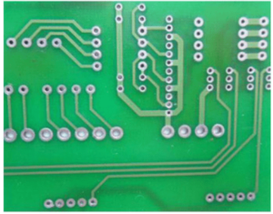
A printed circuit board (PCB) is an essential component in electronic assemblies, providing mechanical support for electronic components and facilitating electrical connections between them. The intricate design of PCBs involves the use of copper conductors to create various features like traces, pads, and conductive planes, all sandwiched between insulating layers. After going through a meticulous fabrication process that includes lamination, plating, solder masks, and silk screen printing, the bare PCB enters the assembly phase where components are soldered onto the board.
Today, the design of printed circuit boards has become a distinct discipline within the electronics industry. PCBs are crucial as they enable electrical interconnections, offer rigid support for components, and provide a compact package that can be seamlessly incorporated into end products. Even the most basic circuit board requires careful design using specialized software, which can guide the process from concept to manufacturing. In this article, we will delve deeper into the meaning of PCBs, their design intricacies, and important considerations for creating effective circuit boards.
The Evolution of PCBs#
Before the advent of printed circuit boards, electronics were assembled using individual wires to connect components, a method that proved impractical as designs evolved to include high pin count components and intricate integrated circuits. The shift to using copper connections on insulating substrates revolutionized the manufacturing processes for circuit boards. Present-day printed circuit boards power an extensive range of devices from smartphones to medical equipment, with advanced HDI designs containing thousands of connections and multiple electrical interfaces.
Types of PCBs#
In addition to the typical rigid substrates used for assembling circuit boards, there are various other types of PCBs that cater to specific requirements:
Single-sided: Features components mounted on one surface, with the back surface typically covered in copper and a solder mask.
Double-sided: Contains components mounted on both surfaces, with each surface serving as a signal layer in the PCB stack-up.
Multi-layer PCBs: Include internal conductive layers for carrying electrical signals between components, with the possibility of single or double-sided configurations.
Rigid PCBs: Constructed and assembled on rigid laminate materials such as FR4-grade epoxy resin-impregnated fiberglass laminate.
Rigid-flex PCBs: Utilize a flexible polyimide ribbon to connect rigid sections for designs requiring movable elements.
Flex PCBs: Comprised of fully flexible polyimide ribbons, offering flexibility for specific applications.
Metal-core PCBs: Employ a metal slab within the core layer, providing enhanced rigidity and heat dissipation suitable for high-power lighting and industrial applications.
Ceramic PCBs: Utilized in applications requiring high thermal conductivity to dissipate large amounts of heat away from components.
Structure and Applications of PCBs#
The performance and reliability of a PCB are heavily influenced by its layer stack-up, which comprises alternating layers of conductive and insulating materials as well as core and prepreg dielectrics. The selection of core and prepreg materials is crucial, particularly in high-reliability applications such as military, medical, and telecom systems, where specific characteristics are required for optimal functionality. Come to PCBPit for pcb making now.