Printed Circuit Boards (PCBs) are the foundation of electronic devices, providing a platform for components to be connected and integrated. Cavity PCBs, also known as recessed PCBs, refer to a specific type of PCB design that incorporates cavities or cutouts that do not completely penetrate the board.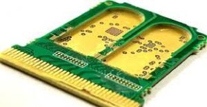
These cavities create recessed areas on the board where components can be mounted, offering several advantages over traditional PCB designs.
Advantages of Cavity PCBs
Cavity PCBs offer numerous benefits that make them suitable for various electronic applications. Let’s explore some of the key advantages:
1. Size and Weight Reduction
By integrating recessed areas into the PCB, components can be mounted inside the cavities, effectively reducing the overall height and size of the product. This compact design allows for more efficient utilization of available space, making it ideal for applications with limited real estate. The reduced size and weight of cavity PCBs contribute to lighter and more portable electronic devices.
2. Increased Assembly Density
The use of cavities on the PCB provides additional space between components, allowing for increased assembly density. This density enhancement enables more components to be mounted on the board, leading to higher functionality in a smaller area. Cavity PCBs are particularly beneficial when designing complex electronic systems with multiple components that require close proximity to each other.
3. Improved Performance and Reliability
The separation between components achieved through recessed cavities reduces the interference that can occur between closely positioned elements on a PCB. With proper spacing and isolation, electrical signals are less likely to interfere with each other, resulting in improved signal integrity and overall performance. Additionally, the reduced proximity of components helps dissipate heat more efficiently, reducing the risk of overheating and enhancing the reliability and lifespan of the electronic device.
4. High-Speed and High-Informatization Compatibility
As technology advances, electronic devices increasingly require high-speed and high-informatization capabilities. Cavity PCBs are designed to meet these requirements by allowing for the implementation of complex integrated circuits, high-speed connectors, and advanced signal processing technologies.
These PCBs offer improved transmission characteristics, reduced signal degradation, and minimized electromagnetic interference, making them suitable for a wide range of high-performance and data-intensive applications.
5. Diverse Application Possibilities
Cavity PCBs find applications in various industries and electronic systems. Some common areas where these PCBs are utilized include:
- RF and Microwave Systems: Cavity designs are crucial in RF and microwave applications, where signal integrity and isolation are critical. The design allows for precise control of electromagnetic waves, minimizing interference and optimizing performance.
- Telecommunications: With the growing demand for smaller and more powerful communication devices, cavity PCBs enable the integration of complex wireless communication technologies into compact form factors.
- Automotive Electronics: Cavity PCBs are instrumental in automotive electronics, enabling the implementation of advanced features such as collision detection, driver assistance systems, and communication modules within restricted space.
- Power Amplifiers: In high-power applications, heat dissipation is crucial to maintain optimal performance. Cavity PCBs provide a solution by creating recessed areas that facilitate efficient heat management and cooling.
- High-Speed Computing: Cavity PCBs can support high-speed processor chips and memory modules, ensuring efficient data transmission and processing in modern computing systems.
IPC Standard for Cavity PCBs
The IPC (Institute for Printed Circuits) standard defines three types of recessed cavities for rigid PCBs:
- Type I: Partial Grid Score
In this type, partial grid score lines are applied to one or both sides of the PCB, allowing for the removal of specific areas of the circuit board. The partial grid score lines typically eliminate one or more corners to create a recessed area without completely penetrating the board. - Type II: Partial Punch
Type II cavities are created by punching recessed areas on one or both sides of the PCB. The punch process removes the material required to create the cavities without penetrating through the entire board. - Type III: Routed Cavity
Routed cavities, also known as milled cavities, are created using precision routing machines. The routing process selectively removes material, creating cavities without penetrating through the entire board.
Conclusion
Cavity PCBs provide significant advantages in reducing product size, increasing assembly density, improving performance and reliability, and meeting the requirements of high-speed and high-informatization applications. With their versatile application possibilities across industries such as RF and microwave systems, telecommunications, automotive electronics, power amplifiers, and high-speed computing, cavity PCBs continue to catalyze advancements in electronic devices. These specialized PCBs enable designers to optimize layouts, minimize interference, and enhance overall system performance in a compact and efficient manner

Humanizey Review: I Tested Everything Out
Humanizey Review: I Tested Everything Out AI writing tools have changed the way we create content. They’re fast, smart, and efficient. But even the best

AllPCB Review: Can We Trust It?
AllPCB Review: Can We Trust It? In this in-depth review, we’ll examine AllPCB’s strengths, weaknesses, and whether it deserves your trust. We’ll also explore PCBPit,

PCBgogo Review: Is It A Good PCB Manufacturer?
PCBgogo Review: Is It A Good PCB Manufacturer? In this in-depth review, we’ll dissect its strengths, weaknesses, and alternatives—with a focus on PCBPit, a rising

NextPCB Review: Does It Really Work?
NextPCB Review: Does It Really Work? Choosing a reliable PCB manufacturer is critical for bringing your electronics projects to life. NextPCB has been a prominent