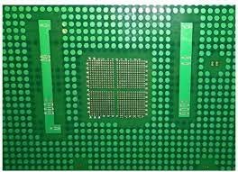
Copper thieving refers to the strategic inclusion of non-functional copper geometries, such as dots, squares, or continuous planes, to areas of a PCB’s surface which lack copper features. This additional copper serves to balance the overall distribution without being electrically connected to the circuit, ensuring it does not impact the board’s operational performance.
Association with Copper Pour Techniques
Similar to copper thieving, the copper pour technique is employed to distribute copper evenly across the PCB, most commonly forming ground and power planes. These planes can enhance signal quality, minimize electromagnetic interference (EMI), and help with thermal management.
Combining copper pours with copper thieving can optimize the PCB’s copper balance, such as utilizing thieving around densely-packed components and applying copper pour in the remaining areas to ensure a uniform distribution.
Benefits of Copper Thieving
Uniformity in Electroplating
Copper thieving is integral in achieving uniform electroplating on PCBs, particularly for the internal vias and through-holes. Without a balanced copper layout, electroplating can lead to excessive copper in sparsely populated areas, raising the risk of short circuits, or inadequate copper near densely-packed regions, which can affect connectivity and degrade the quality of solder joints. Copper thieving circumvents these issues by evenly distributing the electroplating current over the board surface.
This is particularly vital in high-power applications or where large currents traverse the PCB, as copper anomalies can lead to significant malfunctions.
Enhanced Solderability
Employing copper thieving contributes to a dependable copper foundation for soldering components, which is pivotal for solid solder joints and enduring board performance. Insufficient copper can result in weak joints, while too much can make them brittle. Copper thieving assists in maintaining an optimal copper layer thickness to avert these issues.
Maintaining Signal Integrity
In applications involving high-speed digital signals or RF circuits, preserving the PCB’s transmission line impedance is crucial to avoid signal loss or corruption. Copper thieving promotes impedance consistency by standardizing copper thickness, thereby preventing signal reflection and data accuracy problems.
Click here to get all-in-one solution at PCBPit >>
Implementation Considerations for Copper Thieving in PCB Layouts
When integrating copper thieving into PCB designs, certain best practices must be considered. Firstly, thieving patterns need to be designed to ensure they do not compromise signal integrity, affect solderability, or weaken structural integrity. Additionally, they must remain electrically isolated from active circuits to avoid creating unintended conductive paths. Finally, strategic placement of thieving is essential, especially in zones prone to uneven copper distribution, such as regions with limited copper exposure or adjacent to high-component-density areas.

Humanizey Review: I Tested Everything Out
Humanizey Review: I Tested Everything Out AI writing tools have changed the way we create content. They’re fast, smart, and efficient. But even the best

AllPCB Review: Can We Trust It?
AllPCB Review: Can We Trust It? In this in-depth review, we’ll examine AllPCB’s strengths, weaknesses, and whether it deserves your trust. We’ll also explore PCBPit,

PCBgogo Review: Is It A Good PCB Manufacturer?
PCBgogo Review: Is It A Good PCB Manufacturer? In this in-depth review, we’ll dissect its strengths, weaknesses, and alternatives—with a focus on PCBPit, a rising

NextPCB Review: Does It Really Work?
NextPCB Review: Does It Really Work? Choosing a reliable PCB manufacturer is critical for bringing your electronics projects to life. NextPCB has been a prominent