Printed Circuit Boards (PCBs) are the backbone of most electronic devices, connecting components with a series of electrical paths. One crucial but often overlooked component is the PCB Gold Finger. These gold-plated connectors play a vital role in ensuring reliable and efficient connections between the PCB and other components.
The Role and Design of Gold Fingers
Understanding Gold Fingers in PCBs
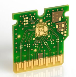
Gold Fingers are thin strips of conductive material, typically gold, found on one edge of a PCB. Their primary function is to provide a robust connection point that can withstand repeated insertion and removal from a mating connector or slot, such as in computer memory and expansion cards.
Why Gold?
The choice of gold for these connectors isn’t arbitrary. Gold offers several benefits:
- Corrosion Resistance: Gold doesn’t tarnish or corrode, which is crucial for maintaining a stable connection over time.
- Excellent Conductivity: Gold’s high conductivity ensures minimal signal loss.
- Durability: Despite being soft, gold’s malleability allows for a certain level of flexibility, making it less prone to cracking or breaking.
The Manufacturing Process
Creating Gold Fingers involves several steps:
- Patterning: The general shape of the fingers is etched onto the PCB.
- Plating: A thin layer of nickel is first plated onto the fingers, followed by a layer of gold. The nickel acts as a barrier to prevent the gold from diffusing into the copper base.
- Finishing: The edges of the gold fingers are often beveled to ensure a smooth insertion into connectors.
Try PCBPit for pcb manufacturing services today >>
Applications of Gold Fingers in Electronics
Where You’ll Find Them
Gold Fingers are present in various electronic devices and components. Some common applications include:
- Computer Expansion Slots: RAM modules and graphics cards.
- Peripheral Connections: Edge connector sockets for printers, modems, and other devices.
- Industrial Applications: Robotics and automation systems often rely on these connectors for reliable communication between components.
Challenges and Considerations in Design
Ensuring Quality and Reliability
The design and manufacturing of PCB Gold Fingers require precision. Factors such as the thickness of the gold plating and the quality of the underlying nickel layer are crucial. Inadequate plating can lead to wear and tear, while excessive plating can increase costs unnecessarily.
Environmental and Cost Concerns
The use of gold, although beneficial for performance, raises concerns about cost and environmental impact. The extraction and processing of gold can be expensive and environmentally damaging. Therefore, striking a balance between quality and these factors is essential.
Try PCBPit for pcb assembly services today >>
Future Trends and Developments
Innovations in PCB Design
The future of PCB Gold Fingers lies in the development of new materials and processes that offer similar benefits at a lower environmental and financial cost. Research into alternative coatings and base metals is ongoing, with the aim of maintaining or improving conductivity and durability while reducing the reliance on gold.
The Role of Gold Fingers in Advancing Technology
As technology evolves, the demands on PCBs and their connectors increase. High-speed data transfer and smaller, more complex devices require connectors like Gold Fingers to be more efficient and reliable than ever. Innovations in this field will directly impact the capabilities of future electronic devices.
Conclusion: Reflecting on the Significance of PCB Gold Fingers
In the intricate world of electronics, PCB Gold Fingers might seem like a small detail, but they are a testament to the marvels of modern engineering. Their design and functionality reflect a harmonious blend of material science, electrical engineering, and practical economics. As we move forward, the evolution of these tiny yet mighty components will continue to shape the efficiency and reliability of the electronic devices that have become integral to our daily lives.
Reflecting on this, one can appreciate the intricate details that go into even the smallest components of our technological world. It challenges us to consider the broader implications of our choices in materials and design, not just for functionality, but for environmental sustainability and cost-effectiveness.
The humble PCB Gold Finger, therefore, is not just a component; it’s a symbol of the ongoing quest for innovation and balance in the ever-evolving landscape of technology.
PCB Ruler: A Comprehensive Guide
PCB Ruler: A Comprehensive Guide What is a PCB Ruler? A PCB ruler is a functional tool made from the same materials as a printed
Thermal Vias: A Comprehensive Guide for PCB Heat Management
Thermal Vias: A Comprehensive Guide for PCB Heat Management Why Heat Management Matters in PCBs Before diving into thermal vias, let’s understand why heat is

PCB Testing Guide: Everything You Need to Know
PCB Testing Guide: Everything You Need to Know This guide will walk you through the essentials of PCB testing, including why it matters, common testing
What Is A Rogers PCB?
What Is A Rogers PCB? If you’ve ever used a smartphone, connected to Wi-Fi, or marveled at satellite communication, you’ve indirectly interacted with a technology