Printed Circuit Boards (PCBs) are the backbone of electronic devices, providing electrical connections and mechanical support for various components. A critical aspect of PCB manufacturing that significantly influences its performance, durability, and functionality is plating.
PCB plating involves the coating of the board’s surface and its holes with a metal layer, which can include copper, gold, silver, or tin, to improve solderability, conductivity, and resistance to corrosion. This comprehensive guide delves into the world of PCB plating, exploring its types, processes, benefits, and considerations.
Understanding PCB Plating
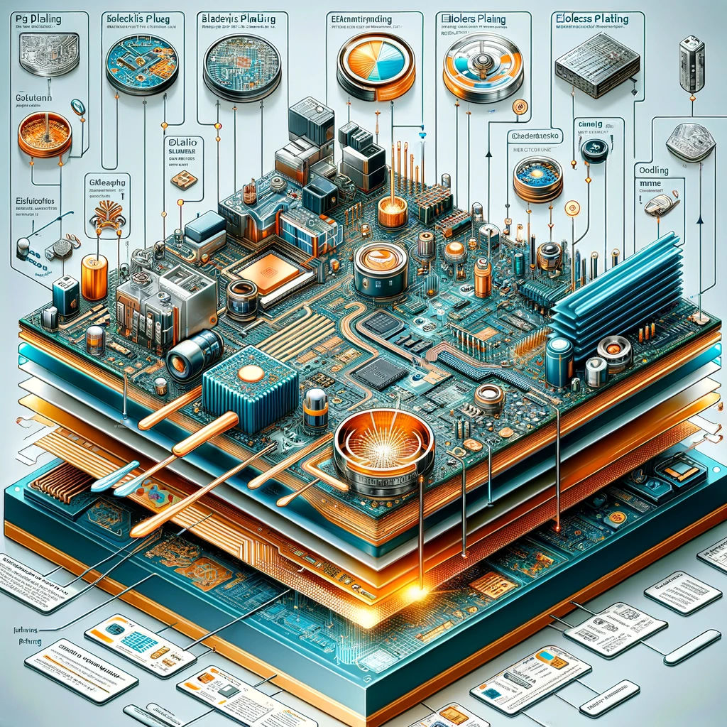
PCB plating is a sophisticated process that enhances the board’s electrical and mechanical properties. It involves the application of a thin metal layer over the base material or copper traces. The primary purposes of plating are to ensure strong solder joints, protect against corrosion, and increase the PCB’s overall lifespan.
Types of PCB Plating
Electrolytic Plating: This process uses an electrical current to deposit metal on the board’s surface. It’s commonly used for adding thick copper layers in through-holes or on the surface to increase conductivity.
Electroless Plating: Unlike electrolytic plating, this method doesn’t require electricity. Instead, it uses a chemical reaction to achieve metal deposition. It’s particularly useful for uniform plating on non-conductive surfaces.
Immersion Plating: This method involves dipping the PCB in a solution containing the plating metal, which chemically displaces some of the surface material with the plating metal. Immersion gold over nickel is a popular choice for its excellent conductivity and durability.
Direct Gold Plating: Directly plating gold onto copper surfaces, this method is less common due to the high cost of gold. However, it provides exceptional corrosion resistance and electrical properties.
The Plating Process
The PCB plating process varies depending on the type of plating being performed but generally includes several key steps:
Cleaning and Preparation: The PCB is thoroughly cleaned to remove any contaminants that could interfere with the plating process.
Catalyzation and Activation: For electroless plating, the surface is treated with a catalytic solution to make it conducive to the chemical deposition of the metal.
Plating: The board is exposed to the plating solution through one of the methods described above, allowing the metal to deposit onto the surface or in the holes.
Post-Plating Treatment: After plating, the PCB may undergo additional treatments such as rinsing, drying, and applying a protective outer layer to enhance durability.
Benefits of PCB Plating
Enhanced Conductivity: Metal plating, especially copper, improves the PCB’s ability to conduct electricity, essential for high-performance electronics.
Increased Durability: Plating protects the PCB from environmental factors like humidity and corrosion, significantly extending its lifespan.
Improved Solderability: A well-plated PCB ensures strong, reliable solder joints by improving the surface’s ability to bond with solder.
Corrosion Resistance: Certain plating materials, like gold, provide excellent resistance to oxidation and corrosion, ensuring the longevity of the board and its components.
Considerations and Challenges
While PCB plating offers numerous benefits, it also presents challenges that manufacturers must address:
Cost: The choice of plating material can significantly impact the overall cost of the PCB. Gold and silver, for example, offer excellent performance but at a higher price.
Complexity: The plating process involves multiple steps and careful control of conditions, making it complex and time-consuming.
Environmental Impact: Some plating processes use hazardous chemicals that require proper handling and disposal to minimize environmental impact.
Quality Control: Ensuring uniform plating thickness and quality across the entire PCB is critical for performance but can be challenging to achieve consistently.
Conclusion
PCB plating is a vital process in the manufacture of printed circuit boards, enhancing their performance, durability, and functionality. By understanding the different types of plating available and their respective benefits and challenges, manufacturers can make informed decisions that optimize the quality and reliability of their electronic devices.
While the process requires careful consideration of cost, complexity, and environmental impact, the advantages of well-executed PCB plating are undeniable, making it an essential component of modern electronics manufacturing.
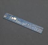
PCB Ruler: A Comprehensive Guide
PCB Ruler: A Comprehensive Guide What is a PCB Ruler? A PCB ruler is a functional tool made from the same materials as a printed
Thermal Vias: A Comprehensive Guide for PCB Heat Management
Thermal Vias: A Comprehensive Guide for PCB Heat Management Why Heat Management Matters in PCBs Before diving into thermal vias, let’s understand why heat is

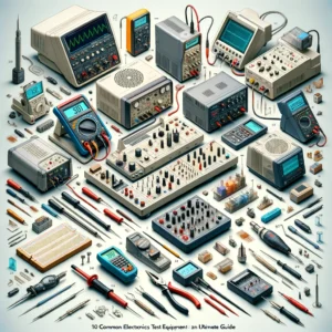
PCB Testing Guide: Everything You Need to Know
PCB Testing Guide: Everything You Need to Know This guide will walk you through the essentials of PCB testing, including why it matters, common testing
What Is A Rogers PCB?
What Is A Rogers PCB? If you’ve ever used a smartphone, connected to Wi-Fi, or marveled at satellite communication, you’ve indirectly interacted with a technology