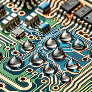
What are PCB Teardrops?
PCB teardrops are small, teardrop-shaped enlargements at the junction where a track (or trace) meets a pad or via on a circuit board (see Figure 1). These are not randomly placed but are carefully designed to enhance the physical and electrical connection between these components.
Significance of PCB Teardrops
- Stress Distribution: The primary purpose of a teardrop is to distribute mechanical stress. When a PCB flexes during assembly or use, stress concentrates at the junctions of pads and traces. The teardrop shape helps distribute this stress more evenly, reducing the likelihood of trace fracture.
- Improved Manufacturability: During the drilling process, misalignment can lead to drill breakouts, where a part of the pad or annular ring is removed. Teardrops increase the amount of copper in the sensitive area, thus reducing the impact of such misalignments.
- Enhanced Electrical Connection: By increasing the copper area at the junctions, teardrops can also improve the electrical connection. This is particularly beneficial in high-frequency PCBs where even minor imperfections can significantly affect performance.
Click to get PCB assembly services at PCBPit now >>
Implementation in PCB Design
Implementing teardrops in PCB design involves a balance between added material and maintaining signal integrity. Modern PCB design software often includes automated tools to add teardrops to a design effectively. The key considerations include:
- Size and Shape: The teardrop must be large enough to provide the necessary strength but not so large as to interfere with nearby traces or components.
- Placement: Teardrops are typically placed at every trace-to-pad and trace-to-via junction.
- Layer Consideration: In multi-layer PCBs, teardrops need to be carefully implemented to ensure they do not interfere with other layers.
Challenges and Considerations
While teardrops offer numerous benefits, they also present certain challenges:
- Space Constraints: In densely packed PCBs, adding teardrops can be challenging without affecting neighboring traces or components.
- Signal Integrity: For high-speed circuits, the change in trace width due to teardrops can impact impedance and signal integrity. Designers need to account for these changes.
- Aesthetic Factors: In some cases, particularly in consumer electronics, the appearance of the PCB might be a consideration. Teardrops can alter the look of the board.
Conclusion
PCB teardrops, though small and often unnoticed, play a crucial role in enhancing the durability and reliability of circuit boards. Their implementation requires a nuanced understanding of both the mechanical and electrical aspects of PCB design.
As technology advances and PCBs become more complex and miniaturized, the role of features like teardrops in ensuring the longevity and performance of electronic devices becomes increasingly vital.
PCB Ruler: A Comprehensive Guide
PCB Ruler: A Comprehensive Guide What is a PCB Ruler? A PCB ruler is a functional tool made from the same materials as a printed
Thermal Vias: A Comprehensive Guide for PCB Heat Management
Thermal Vias: A Comprehensive Guide for PCB Heat Management Why Heat Management Matters in PCBs Before diving into thermal vias, let’s understand why heat is

PCB Testing Guide: Everything You Need to Know
PCB Testing Guide: Everything You Need to Know This guide will walk you through the essentials of PCB testing, including why it matters, common testing

What Is A Rogers PCB?
What Is A Rogers PCB? If you’ve ever used a smartphone, connected to Wi-Fi, or marveled at satellite communication, you’ve indirectly interacted with a technology