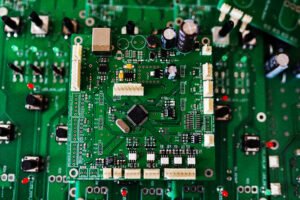
What Is Via in Pad?

In the ever-evolving landscape of electronic devices, which are becoming smaller, more complex, and carry an increased functionality demand, PCBs are obliged to facilitate greater routing densities. To address this need, the via-in-pad design is frequently utilized.
This approach positions a via directly beneath a component’s mounting pad on the PCB surface, providing a direct link from the pad to the internal circuit layers, thus circumventing the conventional approach of tracing routes around the pad.
Process of Via-in-Pad Filling
During the via-in-pad technique, the vias are usually infused with non-conductive epoxy, sealed, and then covered with plating material. This practice is instrumental in preventing short circuits or defective solder joints due to solder escaping into the via. Full via encapsulation is critical as it minimizes the potential for void formation and promotes uniform plating. This particular procedure is distinct from “via tenting,” which depends on soldermask application to insulate the via and hinder solder penetration during the assembly process.
Guidelines for Via-in-Pad Design
There are critical considerations to make when integrating the via-in-pad design into a PCB. These considerations encompass selecting the optimal via dimensions to avoid increased resistance or unwanted capacitance, strategically positioning the via to mitigate signal interference and reflections, sizing the annular ring correctly to preserve the via’s electrical and heat dissipation capacity, and crafting the solder mask properly to ensure solder does not creep into the via, which could result in issues such as solder voids or the formation of solder balls.
Click to get PCB manufacturing services at PCBPit >>
Applying Via-in-Pad in PCB Layouts
Is a via-in-pad arrangement always the right choice for every PCB layout? In deliberating on incorporating via-in-pad into your design, ponder the following scenarios:
Enhanced Density
Utilizing via-in-pad design may be advantageous when your objective is to maximize component and trace placement within a confined space on the PCB, thereby diminishing the via count on the board surface.
Better Thermal Management
Via-in-pad designs are adept at dissipating heat from components that generate elevated temperatures, such as power devices, by forming a direct heat conduction path to a copper plane.
Augmented Electrical Performance
Should the goal be to enhance circuit performance electrically, via-in-pad provides a low-impedance path between the component and the PCB’s internal layers.
High-frequency Usage
In high-frequency operations, via-in-pad is beneficial for managing the connection impedance and bolstering signal integrity.
Despite the advantages, via-in-pad design can introduce challenges like increased production complexity, escalated costs, and the risk of thermal strain on components. The appropriateness of via-in-pad design is contingent upon the unique specifications and limits of your particular design.
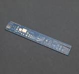
PCB Ruler: A Comprehensive Guide
PCB Ruler: A Comprehensive Guide What is a PCB Ruler? A PCB ruler is a functional tool made from the same materials as a printed
Thermal Vias: A Comprehensive Guide for PCB Heat Management
Thermal Vias: A Comprehensive Guide for PCB Heat Management Why Heat Management Matters in PCBs Before diving into thermal vias, let’s understand why heat is

PCB Testing Guide: Everything You Need to Know
PCB Testing Guide: Everything You Need to Know This guide will walk you through the essentials of PCB testing, including why it matters, common testing

What Is A Rogers PCB?
What Is A Rogers PCB? If you’ve ever used a smartphone, connected to Wi-Fi, or marveled at satellite communication, you’ve indirectly interacted with a technology