When it comes to electronic devices and circuit boards, precision and reliability are paramount. Any deviation from perfection in the manufacturing process can lead to performance issues or even complete system failure. One such manufacturing defect that can plague printed circuit boards (PCBs) is known as "PCB Tombstone."
In this article, we’ll delve into what PCB Tombstone is, why it happens, and how to prevent it from impacting the functionality and reliability of electronic devices.
Understanding PCB Tombstone
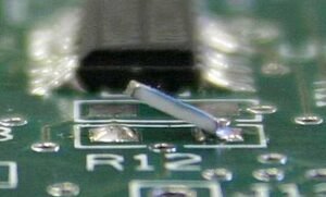
PCB Tombstone, also referred to as “tombstoning” or the “tombstone effect,” is a soldering defect that occurs during the assembly of surface-mount components on a PCB. It gets its name from the visual resemblance of the defect to a tombstone, where one end of the component stands upright while the other end lifts off the PCB, resembling a headstone in a graveyard.
This defect can affect various electronic devices, from smartphones and laptops to automotive electronics and medical equipment. Tombstoning can lead to erratic behavior, intermittent connections, or outright failure of electronic components, causing not only functional but also financial and reputational damage.
Why Does Tombstoning Occur?
To understand why tombstoning happens, it’s essential to look at the soldering process in PCB assembly. Surface-mount components are attached to the PCB using solder paste, a mixture of tiny solder particles and flux. The PCB is then heated, melting the solder paste and creating a secure electrical and mechanical connection.
Tombstoning primarily occurs due to imbalances in the forces exerted on the component during the solder reflow process. Several factors contribute to this phenomenon:
- Imbalanced Thermal Profile: If the PCB experiences an uneven thermal profile during reflow soldering, with one end heating faster than the other, it can result in tombstoning.
- Component Design: Component packages with uneven weight distribution or different thermal characteristics on each terminal are more prone to tombstoning. For example, capacitors and resistors with larger terminations on one end are more susceptible.
- Solder Paste Volume: Incorrect deposition of solder paste can lead to tombstoning. Insufficient solder paste on one pad can cause one terminal to lift while the other stays attached.
- Uneven Pad Sizes: PCB pad sizes should be consistent for both terminals of a surface-mount component. Mismatched pad sizes can induce tombstoning.
- Component Placement: Precision is key in placing components on the PCB. Misalignment during placement can result in tombstoning.
Turn to PCBPit for PCBA solutions now >>
Preventing Tombstoning
Preventing tombstoning is crucial to ensure the reliability and functionality of electronic devices. Here are some strategies and best practices to minimize the risk of tombstoning during PCB assembly:
- Optimize Thermal Profile: Maintain a balanced thermal profile during reflow soldering to ensure even heating of components. Proper profiling of the reflow oven is essential.
- Component Design: Select components with balanced terminal sizes and thermal characteristics. Some manufacturers offer components specifically designed to reduce tombstoning.
- Solder Paste Inspection: Implement quality control measures to verify the correct deposition of solder paste. Automated inspection systems can help detect irregularities.
- Pad Design and Size: Ensure consistent pad sizes for both terminals of surface-mount components. Consult component datasheets for recommended pad sizes.
- Component Placement: Invest in high-precision pick-and-place machines to accurately position components on the PCB. Implement vision systems for real-time placement verification.
- Stencil Design: Optimize stencil design to achieve consistent solder paste deposition. Fine-tune stencil thickness and apertures to match component pad sizes.
- Reflow Process Control: Regularly monitor and calibrate reflow soldering equipment to maintain temperature accuracy and consistency.
- Quality Control: Implement rigorous quality control processes, including visual inspection and automated optical inspection (AOI), to detect and rectify tombstoning defects.
By incorporating these measures into the PCB assembly process, manufacturers can significantly reduce the occurrence of tombstoning and enhance the reliability of their electronic products.
Conclusion
PCB Tombstone is a soldering defect that can plague the reliability and functionality of electronic devices. It occurs when one terminal of a surface-mount component lifts off the PCB during reflow soldering, resembling a tombstone in a graveyard. Tombstoning can lead to performance issues, intermittent connections, or even complete system failure.
Understanding the causes of tombstoning and implementing preventive measures during PCB assembly is crucial for electronics manufacturers. By optimizing thermal profiles, selecting components with balanced designs, controlling solder paste deposition, and maintaining precision in component placement, manufacturers can minimize the risk of tombstoning and ensure the reliability of their electronic products.
In the world of electronics, where precision and reliability are paramount, addressing and preventing tombstoning is a critical step toward achieving excellence in PCB manufacturing and assembly.

Trends and Challenges in PCB Manufacturing for 2024
Trends and Challenges in PCB Manufacturing for 2024 As we move into 2024, the printed circuit board (PCB) manufacturing industry continues to evolve rapidly, driven

10 Best PCB Manufacturers in India
10 Best PCB Manufacturers in India The electronics manufacturing landscape in India has seen a significant transformation in recent years, with Printed Circuit Board (PCB)
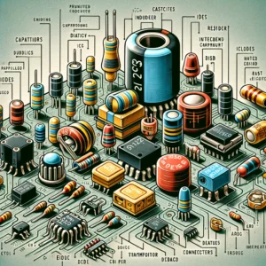
Identifying PCB Components: A Step-by-Step Guide
Identifying PCB Components: A Step-by-Step Guide Printed Circuit Boards (PCBs) are the backbone of modern electronic devices, from simple gadgets to complex machinery. Knowing how
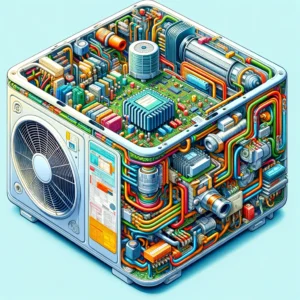
What is PCB in AC?
What is PCB in AC? Air conditioning has become an essential part of our daily lives, providing comfort and a conducive living environment regardless of