In the intricate world of Printed Circuit Board (PCB) manufacturing, the use of photoresist plays a pivotal role in defining the pathways that form the heart of electronic devices. This article unfolds the layers of PCB photoresist, exploring its types, how it’s applied, and why it’s indispensable in crafting precise and functional PCBs.
Whether you’re an experienced engineer, a hobbyist, or new to the field of electronics, understanding the nuances of PCB photoresist is essential for anyone involved in PCB design and production.
What is PCB Photoresist?
PCB photoresist is a light-sensitive material used in the photolithography process to transfer a circuit pattern onto the substrate of a PCB. When exposed to light, the photoresist undergoes a chemical change, allowing selective removal of either the exposed or unexposed areas, depending on the type of photoresist used.
This process creates a protective layer that outlines the circuit pattern, enabling the subsequent etching process to remove unwanted copper, leaving behind the desired circuit pathways.
Types of PCB Photoresist
There are two main types of PCB photoresist: positive and negative.
- Positive Photoresist: When exposed to ultraviolet (UV) light, positive photoresist becomes soluble and can be washed away, leaving the unexposed areas to protect the copper beneath. This type is ideal for detailed circuit designs, as it allows for fine lines and intricate patterns.
- Negative Photoresist: Conversely, negative photoresist becomes hardened when exposed to UV light, making the exposed areas insoluble. The unexposed photoresist is then removed, revealing the copper that needs to be etched away. This type is typically used for simpler designs or where thicker lines are required.
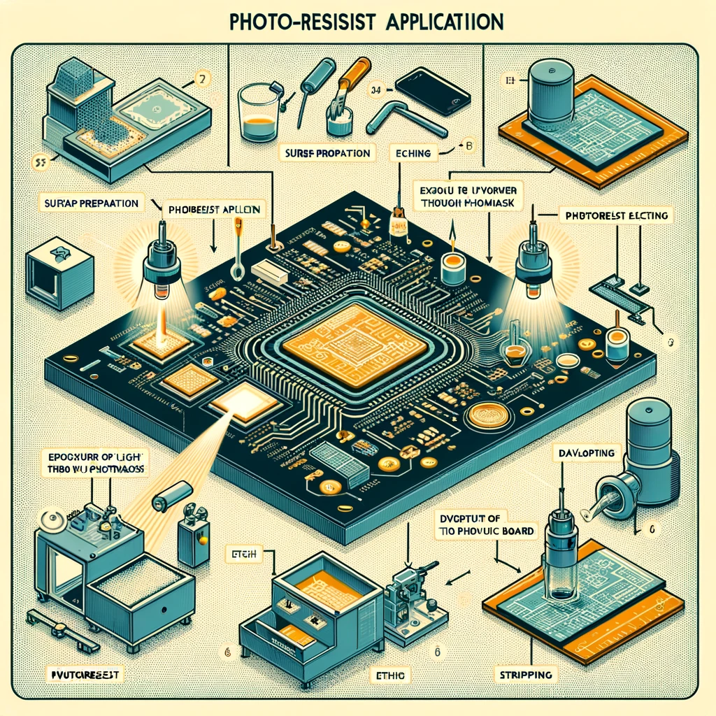
Application Process
The application of photoresist to a PCB involves several key steps:
- Surface Preparation: The copper surface of the PCB is cleaned and prepared to ensure it is free of any contaminants that could interfere with the photoresist adhesion.
- Photoresist Application: The photoresist can be applied in liquid form by spinning or in dry form by laminating. The method chosen depends on the specific requirements of the PCB design and the type of photoresist used.
- Exposure: The photoresist-coated PCB is then exposed to UV light through a photomask, which contains the circuit pattern. This exposure causes the photoresist to chemically change, as described earlier.
- Development: After exposure, the board is developed, washing away either the exposed (for positive photoresist) or unexposed (for negative photoresist) areas, leaving the patterned photoresist on the copper surface.
- Etching: With the photoresist in place, the PCB undergoes an etching process, which removes the unprotected copper, leaving behind the circuit pattern.
- Stripping: Finally, the remaining photoresist is stripped from the board, revealing the completed circuit.
Importance of PCB Photoresist
The importance of PCB photoresist in the manufacturing process cannot be overstated. It directly impacts the precision, reliability, and efficiency of PCB production in several ways:
- Precision: Photoresist allows for the accurate transfer of intricate circuit designs onto the PCB, crucial for the functionality of complex electronic devices.
- Reliability: By providing a protective layer during etching, photoresist ensures that only the intended copper is removed, minimizing the risk of defects.
- Efficiency: Streamlining the manufacturing process, photoresist technology enables rapid production of PCBs, essential in meeting the demands of fast-paced industries.
Challenges and Solutions
While the use of photoresist has revolutionized PCB manufacturing, it also presents challenges, such as the need for precise control over exposure and development processes to avoid defects. Advances in photoresist materials and equipment have addressed many of these challenges, enabling higher resolution, greater consistency, and improved adhesion to various substrates.
Conclusion
The role of PCB photoresist in the fabrication of printed circuit boards is fundamental, shaping the efficiency, precision, and reliability of electronic devices. As technology advances, the continued evolution of photoresist materials and processes will further enhance the capabilities of PCB manufacturing.
For anyone involved in the design or production of PCBs, a thorough understanding of photoresist is indispensable, serving as the foundation upon which successful electronic projects are built.
By publishing this detailed guide on your website, you’ll provide valuable insights into the critical role of PCB photoresist in the electronics manufacturing process, equipping your audience with the knowledge needed to appreciate the complexities and advancements in PCB production.

Humanizey Review: I Tested Everything Out
Humanizey Review: I Tested Everything Out AI writing tools have changed the way we create content. They’re fast, smart, and efficient. But even the best

AllPCB Review: Can We Trust It?
AllPCB Review: Can We Trust It? In this in-depth review, we’ll examine AllPCB’s strengths, weaknesses, and whether it deserves your trust. We’ll also explore PCBPit,

PCBgogo Review: Is It A Good PCB Manufacturer?
PCBgogo Review: Is It A Good PCB Manufacturer? In this in-depth review, we’ll dissect its strengths, weaknesses, and alternatives—with a focus on PCBPit, a rising

NextPCB Review: Does It Really Work?
NextPCB Review: Does It Really Work? Choosing a reliable PCB manufacturer is critical for bringing your electronics projects to life. NextPCB has been a prominent