Introduction
In the engineering world, particularly in the design and manufacturing process of multi-layer Printed Circuit Boards (PCBs), the term “via” has become widespread and essential. A via, a Latin word which means “way”, forms an integral part in the functionality of PCBs. Specifically, it forms the pathway that allows for the transmission of electrical signals from one layer of the PCB to another.
However, for the uninitiated, the term may remain ambiguous. The lingering question remains – what exactly does a via entail in the scope of multi-layer PCBs, and how is it leveraged in designs?
In this article, we aim to unravel the complexities surrounding PCB vias. We will peel back the layers of technical jargon, deliberating on what they are, their functions, and the multiple types available.
What is a Via?
A via is a small drilled hole that passes through two or more adjacent layers, enabling signals and power to travel between these layers. As the circuits between the layers of a multilayer PCB are independent, vias are essential for establishing inter-layer connections.
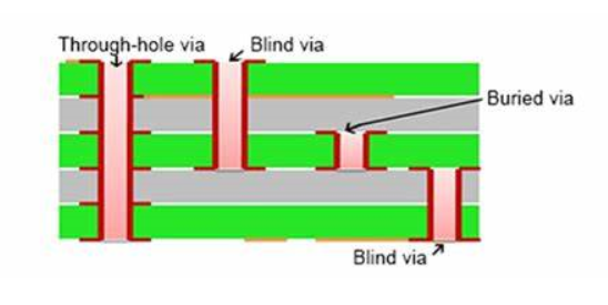
Vias are commonly classified into three types based on their functionality—blind via, buried via, and through-hole via.
Types of Vias
Blind Via
A “blind via” in the context of PCB (Printed Circuit Board) design is a small hole that starts at one surface of the board—either the top or bottom—but doesn’t go all the way through to the other side. Instead, it only connects to one or more layers inside the board. As a result, you can only see and access a blind via from one side of the PCB, since it is not penetrating fully through the entire board.
In the design of PCBs, blind vias have a unique and beneficial usage. One of their main advantages is that they create extra room on the board as they do not traverse all layers. This can be critical in compact designs where space is at a premium. For this reason, you’ll find them frequently used in highly dense circuit assemblies such as BGA (Ball Grid Array) and HDI (High-Density Interconnect) PCBs, where they contribute to achieving a more compact and efficient layout.
Buried Via
A “buried via” is a particular type of via used in Printed Circuit Board (PCB) design. Unlike other vias, it doesn’t reach out to either the top or bottom surface. Instead, it interconnects at least two inner layers of the board, making it invisible from the outer layer. This inward linking nature of buried vias makes them completely hidden from view when you examine the PCB from the outside.
Buried vias play a pivotal role because they facilitate the connection of signals within the inner layers of a PCB. This design can lead to a reduction in signal interference, thereby improving the overall functionality and reliability of the PCB. Given that they enhance the signal integrity and present a more compact layout, buried vias become particularly advantageous in High-Density Interconnect (HDI) PCBs.
In such dense board designs where there’s a critical need to conserve space and maintain high performance, the application of buried vias becomes exemplary.
Through-Hole Via
The “through-hole via” stands as the most frequently used type of via in Printed Circuit Board (PCB) production. It creates a link between the inner and outer layers of the PCB. Unlike other types of vias like blind and buried vias, a through-hole via cuts all the way through the entire board. This is the reason behind its name – it literally creates a ‘through-hole’.
Through-hole vias possess a couple of significant utilities in the scope of PCB manufacturing. Primarily, they serve as channels for internal interconnections within the board, thus allowing electrical signals and power to flow from one layer to another freely.
In addition to this, these vias can also be leveraged as mounting holes for various components of the PCB. This dual functionality adds to their general prevalence in PCB designs and manufacture.
Via Covering Processes
There are three main methods for via covering processes: tenting vias, vias not covered, and plugged vias with solder mask.
Tenting Vias
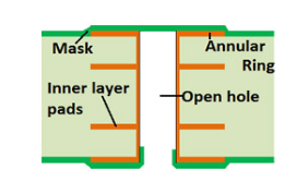
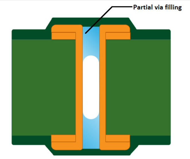
“Tenting vias” is a technique used in Printed Circuit Board (PCB) design to isolate and protect the vias. Here, the annular ring (the visible segment of the via surrounding the hole) is covered with a special substance known as a solder mask. This solder mask functions as an insulating barrier, preventing any unwanted electrical connections from occurring.
Yet, to have an effective tenting of vias, certain factors need to be taken into account. Firstly, it’s important that the annular ring is completely enveloped by the solder mask. Partial covering could leave conductive parts of the via exposed, risking accidental electrical contact.
Additionally, the thickness of the applied solder mask also matters. If it’s too thin, it might not provide adequate insulation, paving the way for potential short circuits. Therefore, one must ensure a thorough and adequately thick solder mask covering to effectively tent vias and protect the circuit.
Vias Not Covered
Choosing “vias not covered” as a design approach for your Printed Circuit Board (PCB) means deciding to leave both the hole of the via and its surrounding ring, also known as the annular ring, exposed. They will not have a layer of solder mask, which typically acts as an insulator. This absence of solder mask sealing leaves the vias open and bare.
This design choice, while it may seem out of the ordinary, has its unique purposes. Uncovered vias are often implemented in cases where debugging measurement signals are needed, allowing for easier access and testing. Additionally, without the insulating solder mask coating, the exposed vias may contribute to enhancing heat dissipation as they provide more surface area.
This can be a boon for circuits generating substantial heat. Despite these benefits, it’s essential to remember that uncovered vias carry a higher risk of unintended electrical connections or short circuits, as the exposed metal could come into contact with unintended conductive materials.
Plugged Vias with Solder Mask
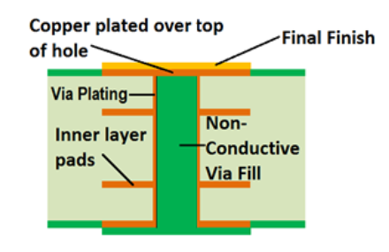
Using “plugged vias with solder mask” is another technique in Printed Circuit Board (PCB) design that provides significant benefits. The process involves filling the via holes with a type of solder mask, which essentially “plugs” or seals them. This design choice intends to enhance the safety and efficiency of the board during its manufacturing and operational phases.
The primary reason for applying solder mask plugs to vias is to prevent what are known as solder balls from forming. These are tiny bits of solder that can cause short circuits during the wave soldering process, a common method for attaching components to the PCB. Furthermore, plugging vias with solder mask helps eliminate flux residue within the via hole, which can lead to other manufacturing and performance issues.
This approach tends to be a necessity in the design of boards that have Ball Grid Array (BGA) or Integrated Circuit (IC) assembly due to the complexity and precision these types of components require. By effectively sealing vias with solder mask, designers can ensure smoother and safer assembly and operation of high-density PCBs.
Conclusion
Unlike through-hole vias, blind and buried vias are only available on boards with at least four layers. The use of blind or buried vias is an effective way to increase the density of multilayer boards, reduce the number of layers, and minimize board dimensions. However, through-hole vias are easier and cheaper to manufacture, making them more commonly used in PCB designs. You can always turn to PCBPit for help.
PCB Ruler: A Comprehensive Guide
PCB Ruler: A Comprehensive Guide What is a PCB Ruler? A PCB ruler is a functional tool made from the same materials as a printed
Thermal Vias: A Comprehensive Guide for PCB Heat Management
Thermal Vias: A Comprehensive Guide for PCB Heat Management Why Heat Management Matters in PCBs Before diving into thermal vias, let’s understand why heat is

PCB Testing Guide: Everything You Need to Know
PCB Testing Guide: Everything You Need to Know This guide will walk you through the essentials of PCB testing, including why it matters, common testing

What Is A Rogers PCB?
What Is A Rogers PCB? If you’ve ever used a smartphone, connected to Wi-Fi, or marveled at satellite communication, you’ve indirectly interacted with a technology