When it comes to designing printed circuit boards (PCBs), one essential concept to understand is stitching vias. These tiny holes play a crucial role in ensuring your PCB works correctly.
In this article, we’ll cover everything you need to know about stitching vias, from what they are to why they’re important and how to use them effectively.
What Are Vias?
Before diving into stitching vias, let’s first understand what vias are. Vias are small holes in a PCB that connect different layers of the board. They act like tunnels, allowing electrical signals, power, and ground connections to travel from one side of the board to another. Vias are like the highways of your PCB, ensuring that everything connects seamlessly.
The Basics of Stitching Vias
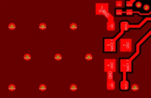
Now that we know what vias are, let’s talk about stitching vias. Stitching vias are a specific type of via arrangement used to create a solid electrical connection between different ground planes in your PCB. In simpler terms, they help ensure that all parts of your board have a consistent and stable connection to the ground.
Imagine your PCB as a city, and the ground planes as the streets. Stitching vias are like bridges connecting all the streets together, making sure there are no isolated or disconnected areas. This is essential for reducing noise, ensuring signal integrity, and preventing interference in your PCB design.
Click to get PCB assembly solutions at PCBPit now >>
Why Are Stitching Vias Important?
Stitching vias serve several critical purposes in PCB design:
- Ground Plane Integrity: They help maintain the integrity of the ground plane, which is crucial for proper circuit operation. A solid ground connection reduces the risk of electrical noise and interference.
- Noise Reduction: By connecting all ground areas, stitching vias help reduce electrical noise, ensuring your signals remain clear and free from distortions.
- Heat Dissipation: In some cases, stitching vias can aid in dissipating heat generated by components on the PCB, preventing overheating issues.
- Mechanical Strength: They also provide mechanical strength to the PCB, helping prevent warping and ensuring it can withstand external forces.
Using Stitching Vias Effectively
Now that we understand the importance of stitching vias, let’s explore how to use them effectively in your PCB design:
- Strategic Placement: Carefully plan the placement of stitching vias. They should be evenly distributed across the board to create a robust ground connection. Avoid clustering them in one area or leaving any parts of the PCB isolated.
- Size Matters: The size of stitching vias matters. Larger vias offer better conductivity and mechanical strength. Consult your PCB manufacturer’s guidelines for recommended via sizes.
- Via Spacing: Maintain an appropriate distance between stitching vias. Too close, and you risk creating an electrical short; too far, and the ground connection may become weak. Follow design rules and guidelines for optimal spacing.
- Layer Connections: Ensure that stitching vias connect all relevant ground layers in your PCB. This typically includes connecting the top and bottom layers to inner ground planes.
- Use Design Software: Utilize PCB design software to help you accurately place and configure stitching vias. Most modern design tools offer features to streamline this process.
- Consider High-Frequency Designs: If you’re working on high-frequency PCB designs, pay extra attention to stitching vias. These designs are more sensitive to signal integrity issues, and proper stitching is critical.
Common Mistakes to Avoid
While stitching vias are essential for PCB design, there are some common mistakes you should avoid:
- Insufficient Stitching: Using too few stitching vias or improperly placing them can lead to ground plane discontinuities and create electrical noise problems.
- Ignoring High-Frequency Needs: Neglecting proper stitching in high-frequency designs can result in signal integrity issues, leading to poor circuit performance.
- Inadequate Sizing: Using vias that are too small may not provide the necessary mechanical strength and conductivity for your PCB.
- Lack of Planning: Failing to plan the placement of stitching vias can result in an inefficient and ineffective grounding strategy.
Conclusion
In the world of PCB design, stitching vias play a crucial role in ensuring the functionality and reliability of your electronic circuits. These tiny connections act as bridges between ground planes, reducing noise, improving signal integrity, and maintaining the overall stability of your PCB.
By understanding the basics of stitching vias, their importance, and how to use them effectively, you can create PCB designs that not only work as intended but also minimize the risk of interference, ensuring your electronic devices perform flawlessly. So, the next time you’re designing a PCB, remember the importance of stitching vias—they’re the key to a well-connected and reliable circuit board.
PCB Ruler: A Comprehensive Guide
PCB Ruler: A Comprehensive Guide What is a PCB Ruler? A PCB ruler is a functional tool made from the same materials as a printed
Thermal Vias: A Comprehensive Guide for PCB Heat Management
Thermal Vias: A Comprehensive Guide for PCB Heat Management Why Heat Management Matters in PCBs Before diving into thermal vias, let’s understand why heat is

PCB Testing Guide: Everything You Need to Know
PCB Testing Guide: Everything You Need to Know This guide will walk you through the essentials of PCB testing, including why it matters, common testing

What Is A Rogers PCB?
What Is A Rogers PCB? If you’ve ever used a smartphone, connected to Wi-Fi, or marveled at satellite communication, you’ve indirectly interacted with a technology